
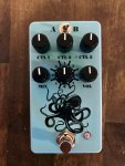
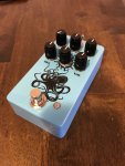
This is my 2nd Arachnid build, my first was the old version with the potentiometer to select patches. This new version with the 8-way switch is much nicer.
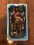
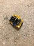
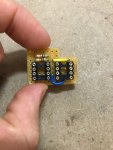
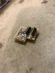
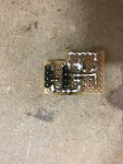
Since PedalPCB hasn't released a dual eeprom board yet, I had to cobble together my own on perfboard. If @PedalPCB does release a dual eeprom board, this would be the configuration I'd vote for, since the most obvious application is to use it on an Arachnid board, and I was able to keep it in a 125B. It was a little tight having the switch at the top under the power jack, but doable.
I included shots of the dual Eeprom daughterboard, and a drawing of the layout. Following info previously provided from PedalPCB, you can select Eeproms by manipulating Pin1. Pin1 low (0v) is activated, Pin1 high (3.3v) is deactivated. As he also noted, fliping the toggle switch doesn't automatically change programs, you have to move the 8-way selector switch before the fv-1 will recognize a program change.
It was tricky soldering the pin headers onto the bottom side of the perfboard, since I had to leave a space between the plastic and the perfobard to get the iron in there. I just noticed that in the pictures that you can see I didn't get solder to fill all the way around on some of them (oops), but the connections all still registered with the multimeter. I used a piece of white foam from Tayda's dip socket packaging to support the cantilevered part of the daughterboard. I had to be careful about the order of soldering (8 way switch, then daughterboard, then mix pot).
For Bank A I used mostly spacialist reverb patches, with a code tweak on the shimmer so that it's only octave up. For the B side, it's a mix of PedalPCB patches (kaleidescope and sample hold), patches I found online, and some I wrote myself. I used my dev board build with exterior eeprom socket to test all the patches and flash the A and B chips.
**EDIT** - the pdf on my original post had an error on the perfboard layout (see p_wats comment on 8/10/2020). I marked up and reattached the pdf.
Attachments
-
 front.jpg708.2 KB · Views: 314
 -
 iso.jpg514 KB · Views: 357
 -
 gut.jpg528.2 KB · Views: 345
 -
 IMG_0730.jpg498.2 KB · Views: 325
 -
 IMG_0731.jpg465.9 KB · Views: 243
 -
 IMG_0732.jpg486.8 KB · Views: 246
 -
 IMG_0733.jpg570.1 KB · Views: 274
 -
FV-1 dual eeprom perfboard layout -rev 8.10.2020.pdf346.3 KB · Views: 125
Last edited:
