aienco
Member
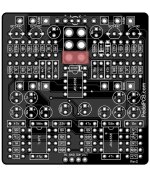
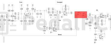
I was wondering if someone would be good enough to point me in the right direction? Through purchasing the wrong switch and soldering and un soldering it, I have totally destroyed the bottom two switch pads. The others are ok and as far as I know, should work. I have looked at the circuit and I can sort of work out where the top four lead, but the bottom two I am having trouble with. Please see pics. I have the correct switch now, but I can't get it to work because of these two pads. Being in Australia, I normally buy two boards for times like this. This time I decided not to?? So I don't want to wait 6 to 8 weeks for another board to come to me, I would like to have a go and seeing if I can save this?
Any guidance would be greatly appreciated.
So I don't want to wait 6 to 8 weeks for another board to come to me, I would like to have a go and seeing if I can save this?Any guidance would be greatly appreciated.