I/O PCB Wiring Diagram

parblar

New member
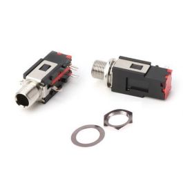
Thought using all pcbs would be easy enough but I’m getting zero audio passing through my spirit box and I’m using all PedalPCB supplied PCBs from my input, board, foot switch and output. I’ve reflowed my solder and my LED lights up but that’s it so far for me today. I’ve confirmed my diagram of the foot switch pcb is correct but there isn’t one of the I/O to compare against.
 

Attachments

  • 71D54A21-AEE8-4388-A88F-6EA1EBAAF300.jpeg
    71D54A21-AEE8-4388-A88F-6EA1EBAAF300.jpeg
    899.5 KB · Views: 17
If you have a DMM plug a cable into the input jack and check continuity from the tip of the jack to the In pad of the I/O board.

Do the same thing for the output jack / Out pad of the I/O board.

I've never used the plastic sleeve jacks so I'm not sure if the pinout of the lugs is the same.
 
I've a question on these as well sir. It seems that the + / - pads are reversed from the main board, or you have to mount it solder-side up? (I'm going by memory).

I like them for BBing !
IMG_4631.jpeg
 
I've a question on these as well sir. It seems that the + / - pads are reversed from the main board, or you have to mount it solder-side up? (I'm going by memory).

I like them for BBing !
Well I thought maybe it was supposed to reverse but then the drilling template has the power in a straight line with the input and output. The three prongs only fit one way there to make them all at the same height and same side of the board but maybe I’m upside down...
 
Well I thought maybe it was supposed to reverse but then the drilling template has the power in a straight line with the input and output. The three prongs only fit one way there to make them all at the same height and same side of the board but maybe I’m upside down...
The DC jack only fits one side ( I tried that ;) )
 
Back
Top