SOLVED Kliche No Sound

Mike52

Active member
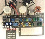
This is aimed at the PedalPCB administrator. Finished a Kliche and, of course, it doesn't work. I get no sound in bypass and an open channel sound (the hum you get from a hot 1/4 jack when you touch it) when engaged and the LED works as it should. So the troubleshooting phase starts now, I guess. Can you send me trace diagrams for the circuit so I can begin testing continuity for all the parts? I believe traces are on both of the sides and I'd like to trace the signal as efficiently as I can while I dissect where I went wrong.

Thanks
 
Last edited:
You can trace it via the schematic. DO you have an audio probe? I would also check this out while you wait for others to chime in.
 
You can trace it via the schematic. DO you have an audio probe? I would also check this out while you wait for others to chime in.
Well, yeah, but its maybe a bit more confusing that way. I like to check continuity from the backside of the board (and that tells only part of the story) and I don't want to be flipping the board all the time trying to determine which component I'm actually testing at the moment. (That would actually be a cool feature if the backside of the board included the component identifier, but oh well.) Basically I'd really like to minimize my handling of the PCB while I'm troubleshooting since that too can lead to problems.

Thanks for the link. I had not seen that one.

Yes, I do have an audio probe.
 
Last edited:
I see what you mean especially for the caps. If you've got the build doc you can look at both the board and schematic pages to check continuity.

I would check out that link. Also, please send pics of both sides of the board. We may be able to see something you don't.
 
+1 to using the schematic
By front, I assume you mean the side with the components? It's easier to probe it on this side since it is usually facing you, so it's unclear to me why you prefer to do it on the backside (not that you need to justify it, I'm merely suggesting that you might be making it harder than it needs to be).
 
Last edited:
+1 to using the schematic
By front, I assume you mean the side with the components? It's easier to probe it on this side since it is usually facing you, so it's unclear to me why you prefer to do it on the backside (not that you need to justify it, I'm merely suggesting that you might be making it harder than it needs to be).
Thanks. I prefer to check continuity from the backside. Its just cleaner. Very easy to inadvertently touch the DMM probe to the clutter of components on the PCB face. It's just a preference.
 
I see what you mean especially for the caps. If you've got the build doc you can look at both the board and schematic pages to check continuity.

I would check out that link. Also, please send pics of both sides of the board. We may be able to see something you don't.
Thanks. I will post a pic if I get a chance. I've been on a bit of a losing streak so am cynically not surprised that it didn't work the first time. I'll do some cleanup work on it tonight (there are a few solder joints I'm not happy with) and then start a troubleshoot checklist and go from there. I've got a sinking feeling that there may be a burned trace there so that would necessitate running a jumper somewhere on the circuit.

Curious, are folks here testing their pedal after soldering every component? Is there a testing phase, or phases, that you use at each phase of the build. I've done that with amplifiers and it sure makes for a stress-less initial powerup. But not sure how to do it when it comes to something as small as a pedal? I did something similar on my first pedal (isolated and tested the power section for supply voltages at key points) but eventually I quit messing with that. Seems like it would be pretty critical for the Klon though.
 
I think you'll find it runs the spectrum. Some of us "box it then rock it" (I'm in this camp), and others test beforehand.

There is a PCB that is made for testing before you box it:

Auditorium Test Platform - PedalPCB.com
Yeah, I"ve seen that. I've thought about buying one but I am just barely committed to this hobby, to be honest. I swear that every pedal I build is the last one I'm gonna build. I think I've broken that promise nine times at this point. Ha.

Another curious question. PedalPCB has two discreet pads on their boards that don't go to anything. They don't really say what those holes do. Anyone know why they are there? Are they testing points of some kind? You can actually see them within space for the TCI044S and the second TL072 ICs if you look closely. Actually, you can also see one next to C7(82n) in the picture provided by PedalPCB.
They'll be vias routing a trace to another layer when your designing pcbs traces can't cross over so you'd use vias for that and longer traces etc

 
As suggested pictures please! I just successfully put together a Kliche after a losing streak of troubleshooting issues myself. Happy to help if I can. If you have a probe then use it! I just use a breadboard with a spare jack, capacitor, test lead, and my guitar. Not trying to be patronizing but doublecheck the orientation of your ICs. I noticed it was a bit confusing when I built the kliche because they didn't all face the same way.
 
For what it's worth, here's a pic of the board. I think pictures make it easier to note the value of these 1% resistors, so that's even helpful to my old eyes. The ICs are easy to screw up, but in this case I oriented them correctly. Last night I cleaned up a couple of suspect solders (and I think its possible I've got a burned solder pad on one of them so we'll see how that works out). I will trace the board later today for continuity but won't be able to add power to it until I get home tonight. I'm sure this will be a long slog.

board.jpg
 

Attachments

  • board.jpg
    board.jpg
    224.4 KB · Views: 10
Last edited:
Yeah, they are. They sort of have a bulbous outcropping on the positive leg and, you can't see it from the pic, the + symbol points to that leg. In this picture, the positive is on top.
 
Purely speculation here, but I've read that insulated jacks can cause grounding issues. Could this be a factor here?

Insulated vs non-insulated jacks | PedalPCB Community Forum
I have a whole bag of them (drunk shopping Tayda, oops) and had never heard that they can cause grounding problems. I'll read the thread. Thanks!

If that were the case, what would I do. Would I ground both together and run an extra ground to the case? Is that what he's describing below? (the noise characteristics I described in the OP sorta support grounding issues, right?)
Screenshot.png
 
Last edited:
I think since the jack issue described is an enclosure grounding issue, it would be apparent if the pedal works outside the enclosure, but then doesn't in the enclosure.

Then again, I could be totally confused--I am not speaking from experience here, only going by what's in that thread. The reason I brought it up in the first place is that I'm not used to seeing those kind of jacks, and it triggered a thought that maybe it's related, but I could be way off base.
 
I think since it's an enclosure grounding issue, it would arise if the pedal works outside the enclosure, but then has issues in the enclosure.

Then again, I could be totally confused--I am not speaking from experience here, only going by what's in that thread. The reason I brought it up in the first place is that I'm not used to seeing those kind of jacks, and it triggered a thought that maybe it's related, but I could be way off base.
I removed the guts from the enclosure anyway to debug it so it doesn't cost anything to power it from my breadboard platform and run a signal through the PCB. This is good, it's giving me at least easy ideas to try. Thanks
 
Back
Top