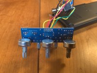
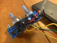
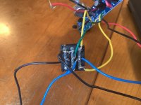
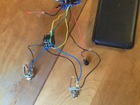
No signal at input w/ Probe

pedal_donny

New member
I have signal through the pedal with the pedal off. No signal with the pedal on. I attached my audio probe to chase through where I lose signal and I don't have any signal with the pedal on right at the input (at the jack). What would that be indicative of? I can touch the end of the probe with my finger and get sound while the pedal is on, but I can't get anything from any part of the pedal.

Before having no signal, I had crazy signal (it's a fuzz factory). I had just plugged the pedal in after finishing it without having cleaned the pcb yet. I had thought something was screwed up, but it's probably just inherent to being a fuzz factory. I cleaned the board with electrical cleaner and a toothbrush and now no signal.

I've built a couple of pedals and successfully chased down some issues with the probe. I'm not 100% inexperienced, but still pretty green.

Thanks.
 
I’ve been wiring this way. It all gets the job done.
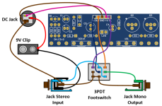
Thanks Jimilee. Are you saying you wire per the sketch I posted in Post #6?

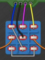
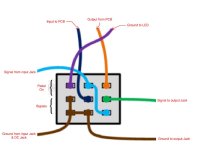
I didn't know how a 3PDT switch worked, but the diagram at the bottom of this was very helpful: 3PDT Switch Sketch . With that in mind, I'd think you could wire the switch in several different ways as long as you ultimately bypass or complete the circuit. The layout from Tayda appears to do that (see the below diagram). It was helpful to understand that the center row is common to both bypass and pedal on positions. The bypass position links the bottom two terminals in each row and the pedal on position links the top two terminals in each row.

All that in mind, I think my problem must be related to something else. Is it possible to lose ground in the on position? I'm just trying to think of why I would lose signal at the input jack with the pedal in the on position.

Sorry to be argumentative. I'm just trying to understand how this works and not go down an empty rabbit hole. I'm an engineer, just not an electrical.
Pedal Switch Diagram.jpg
 
Thanks Jimilee. Are you saying you wire per the sketch I posted in Post #6?

I didn't know how a 3PDT switch worked, but the diagram at the bottom of this was very helpful: 3PDT Switch Sketch . With that in mind, I'd think you could wire the switch in several different ways as long as you ultimately bypass or complete the circuit. The layout from Tayda appears to do that (see the below diagram). It was helpful to understand that the center row is common to both bypass and pedal on positions. The bypass position links the bottom two terminals in each row and the pedal on position links the top two terminals in each row.

All that in mind, I think my problem must be related to something else. Is it possible to lose ground in the on position? I'm just trying to think of why I would lose signal at the input jack with the pedal in the on position.

Sorry to be argumentative. I'm just trying to understand how this works and not go down an empty rabbit hole. I'm an engineer, just not an electrical.
View attachment 44730
Yessir, post #6 was what I was referring to. The 3pdt, top top row connects to the middle row when it’s on. In the off, the bottom connects to the middle. I would agree with you, if you have bypass, then it should work in the on position. That being said, your description is consistent with a cold solder joint. The first step would be to make sure all of your values are correct and then reflow your solder joints.the resistor next to Q2, for example, you can still see the solder pad on the top of the board, unlike the others I can see.
 
Last edited:
Back
Top