Cybercow
Well-known member
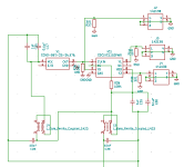
OK, I was able to get some testing time in and found that it does work for the MN30xx series.
And please note that I corrected my comment above - #56
When I tried an MN3102 and an MN3207 I get no sound. Toggle is in the correct position. Haven't measured any voltages yet cuz I was too excited to share what I found so far. More info as it arrives.
EDIT - 9:13pm May 30, 2025
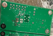
Since burning up one clock chip already, note that the above mentioned test with the MN3102/MN3207, I had power applied for only a moment to do a quick test. After getting no sound from three attempts at getting sound thru the MN3102/MN3207 test, I swapped things back over to test the MN3101/MN3007 chipset and got sound. So I reversed the setup again back to the MN3102/MN3207 test and got no sound. I did NOT unplug the power this time. And by the time I reached over for my DMM probes and brought them to the test board, the MN3102 clock chip opened a small fissure and belched out the tiniest puff of smoke.
With now two burned up clock chips, I figure it's time for me to take break from it this weekend and start fresh on Monday.
FWIW, I know all of my clock and BBD chips are good because I successfully tested them in working circuits. They're too expense to not test for fakes. Still, I'm OK with sacrificing a couple towards this goal. The outcome might benefit the pedal building community.
Last edited:


