Issues with a build of Chuck's Cobalt Drive

devilmollusk

New member
I've been through several iterations trying to build a version of Chuck's Cobalt Drive mod. This version is closest yet. I get signal through the first op amp stage, and the Q1is nicely balanced (~10mV at Q1-D). I get signal all the way through C2, and then nothing. There is connection from Q2->R3, but no audible signal. Also the reading at Q2 are really bizarre. I've tried a few different transistors (I'm using 2SK193s), and so far the readings at Q2 are G=221mv, S=412mv, D=1.86v. I've attached images of the schematic and the PCB layout. Any help would be appreciated!

Screenshot 2026-03-13 at 4.31.29 PM.png Screenshot 2026-03-13 at 4.29.12 PM.png
 

Attachments

  • IMG_3282.jpeg
    IMG_3282.jpeg
    386.9 KB · Views: 32
  • IMG_3279.jpeg
    IMG_3279.jpeg
    514.8 KB · Views: 33
The drain voltages on Q1 & Q2 should be about 8.4V because Q5-B and Q6-B should be Vcc - Vbe. Q5-C and Q6-C should be close to Vref.

Make sure the 2SK193s are oriented correctly, Did you test them before installing?

Make sure Q6 is 2N5087 and that it is making good contact in the socket. IC sockets are not the right size for transistor leads. The leads fit loosely and don't always make good contact.

We'll assume for the moment that the board routing matches the schematic exactly and there are no assembly errors.
 
Ok, I've made sure everything is well seated and double checked orientation. I also replaced Q2 and Q4 with transistors that are very closely matched (all about ~390 hFE). Here are readings:
Q1: 8.66, 4.98, 3.9
Q2: 9.30, 4.98, 3.65
Q3: 9.14, 5.26, 4.29
Q4: 9.3, 5.28, 4.81
Q5: 9.3, 8.6, 2.92
Q6: 9.3, 9.1, 4.8
Q7: 9.3, 4.4, 4.25
 
Are the readings for the JFETs D-S-G?
Are the readings for the BJTs E-B-C?
Complete information is good.

Q1-S & Q3-S are connected together. Why are their voltages different? Same goes for Q2 & Q4.

Q5-C and Q3-G should be the same voltage because Q3's gate current is essentially zero.

3 questions:
What kind of DMM are you using?
What was the setting of the GAIN knob when you made these measurements?
Does the voltage on Q5-C change when you turn the GAIN knob?

If you are using a cheap DMM with a 1M input resistance, it can throw the measurements off.

I just noticed that according to your schematic, the GAIN pots are wired backwards. Pin 3 is at full CW rotation and should be connected to pin 2. You show pin 1 connected to pin 2. same story for VR1B.
 
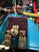
Apologies for the lack of specifics. Here are the readings again, as validated on 2 separate DMMs (AstroAI DM6000AR and OWON HDS272S)
But before I share, I noticed a few issues as I was going along more carefully:
1. I was reporting the names of the transistors wrong. The order I was measuring was L->R for the FETs on the board, so the numbering should be 1,3, 2, 4...
2. Also as I was measuring and double checking I realized that the 2N5087 I'm using for Q5 and Q6 were potentially in backward. I'm not sure how to read this, but here is the datasheet: https://www.onsemi.com/download/data-sheet/pdf/2n5087-d.pdf. It appears that pin 1 is the emitter, however In my schematic pin 3 is marked as the emitter. I must have used a bad 2n5087 symbol (and footprint). I can fix that, but I also rotated the transistor.

Here are the new readings (and yes, the gain knob (also wired backwards, thank you for that catch) affects Q5 C but only a few mA (~5))

Here are the new readings:
Q1 D: 3.9, S:4.99, G:8.66
Q3 D: 3.65, S:4.99, G:9.3
Q2 D:4.5, S:5.7, G:9.3
Q4 D: 4.83, S: 5.23, G:9.3
Q5 C: 4.7, B: 8.68, E: 9.3
Q6 C: 4.85, B: 9.3, E: 9.3.
Q7 C: 9.3, B: 4.26, E: 4.49

Also I'm now getting low volume coming out of the output. The gain knob turns it from audible to nothing, so yeah, progress!

Thanks.
 
You have Q1-Q4 D & G swapped in your measurements.

The DMM is slightly loading the measurements at Q1-G, Q2-G & Q7-B, but we can correct for that.

Looks like there is flux reside on the board. If so, clean that off.

Your schematic has Q5 E&C swapped. Same for Q6. The datasheet is 100% clear to me on which pin is which.

You have C19 hooked up incorrectly. Take another look at the Cobalt schematic.

Check the voltage on U1-6.
 
Got it, will make sure I correct for future measurements.
I'll clean the flux off and try again in a bit.

Your schematic has Q5 E&C swapped. Same for Q6. The datasheet is 100% clear to me on which pin is which.
This is what I meant when I said:
It appears that pin 1 is the emitter, however In my schematic pin 3 is marked as the emitter. I must have used a bad 2n5087 symbol (and footprint). I can fix that, but I also rotated the transistor.

You have C19 hooked up incorrectly. Take another look at the Cobalt schematic.
D'oh! Nice catch, have fixed that in kicad

U1-6: 8.69v
 
Back
Top