Can anyone see any issues with this schematic?

JamieJ

Well-known member
This basically the Sandspur schematic with the input cap on a switch with 1u and 47n, the 470r on a switch with a 1k plus a switch to choose between two bias pots. One would be a trimmer. Then before the output volume pot I have added a AMZ tone control with mids and volume recovery by a LPB circuit.

Can you see any issues here that I have messed up with?
 

Attachments

It is a LED indicator to show a change of bias pot combined with SW2&3. That would be a 3pdt.
 
Last edited:
OK, you asked...

Other than being a tangled mess? If you untangle the wires, it will be much easier to read and much easier to see the redundancies in the switching.

Just to be clear, SW2, SW3 & SW4 are ganged together? If so, you don't need both SW2 & SW3, one will suffice for selecting a bias pot.

Same goes for the two parts of SW5, you can use a single pole for selecting R3 or R23. What is the purpose of SW5? Is it a volume boost?

Why two VOL pots?

You might need to fiddle the biasing of Q3 to maximize headroom. But then, you really don't need Q3, at least you don't need any gain recovery. There is a HUGE signal at Q2's collector, but you divide it way down with R3, R23 and the bias pots. If you rearrange R3, R23 and the bias pots, you won't need Q3, or you can make Q3 an emitter follower.
 
Thanks for the rinsing Chuck 🤣

It’s my first attempt at drawing up a schematic. Thank your for you comments.

I based it on the two schematics pictured from FuzzDog.

Yep - SW5 is a boost. I thought it would get too much of a volume drop from adding just a tone control so I wanted it to have a boost afterwards.

I have built this with the PCBs but it was a nightmare to wire so I wanted to see if I could make a PCB. All a nice and steep learning curve which is great.
 

Attachments

  • B70C4560-3BC2-4684-81B2-BE3AA9B6932E.jpeg
    B70C4560-3BC2-4684-81B2-BE3AA9B6932E.jpeg
    92.5 KB · Views: 10
  • 9E7A7206-0AA3-403A-B244-357032E61484.jpeg
    9E7A7206-0AA3-403A-B244-357032E61484.jpeg
    123.9 KB · Views: 10
Last edited:
DANG!
I love this — the hot mess, the cleanup by circuit-custodian nonpareil CDB...


I've been working on a wigged out Rangemaster-Dizzy combo for a while now... I should pester Chuck to peruse it once I think it's close to being ready...

Despite this gust of inspiration to fill its sails, my RD is dry-docked for the moment as I tend to other urgent matters.
 
I've checked my Schematics 101 doc and boiled it down to the following, in hopes it helps JamieJ and anyone else starting out drawing schematics. Take it with a grain of salt, there are many ways to skin a schematic and everyone develops their own druthers.


The following ideas are mainly from Olin Lanthrop, but a few others added, that I've gleebed from the net and condensed whilst trying to better fathom the art of the schematic myself:

1. Use component designators
instead of second 10 kΩ resistor from the left by the top pushbutton, use designators R1, R5, Q7, etc.


2. Clean up text placement
Vertical text looks awkward and makes a schematic hard to read.

3. Basic layout and flow
In general it is good to put higher voltages towards the top, lower voltages towards the bottom, and logical flow left to right when possible.
Power connections should go up to positive voltages and down to negative voltages.
Common sub-circuits can be drawn similarly most of the time; if they look visually different every time, it will take others longer to understand your schematic. Ex: a common emitter amplifier.

4. Draw pins according to function
Show pins of ICs in position relevant to their function, not how they stick out of the chip. Try to put positive power pins at top, negative power pins (usually grounds) at bottom, inputs at left, and outputs at right. Note that this fits with the general schematic layout as described above. Again, not always possible.

5. Direct connections, within reason
Clarity: Spend some time with placement reducing wire crossings and the like. A direct connection line isn't always feasible. Help people understand the circuit easily, not make them figure it out despite the schematic.


6. Design for regular size paper
The exact size of "regular" is a little different all around the world, but all are easily held in front of you or can be placed on your desk; and on the computer screen at about the same size. Try to avoid having to scroll a page to see detail.
Breaking the schematic into multiple pages is okay.

7. Label key nets
If a net is broken up into visually unconnected segments, then you absolutely have to let people know the two seemingly disconnected nets are really the same. Different packages have different built-in ways to show that. Use whatever works with the software you have, but in any case give the net a name and show that name at each separately drawn segment. Clarity, use little "jump point" markers or whatever if able or deemed necessary. Multiple uses of the variable symbol should refer to the same variable.

For example, seeing that a net is called "5V" could help a lot in understanding the circuit. Many short nets don't need a name or clarification, and adding names would hurt more due to clutter than they would illuminate. Again, the whole point is clarity. Show a meaningful net name when it helps in understanding the circuit, and don't when it would be more distracting than useful.

[Short names rule, but make sure they are descriptive. Don't use "Vcc2" when "12V" is the power running the board derived from an adjustable regulator.]


8. Keep names reasonably short
Clarity. No names is no information, but lots of long names are clutter, which then decreases clarity. Ex "CLOCK", "CLK", or "8MHZ" would convey the same information.
See the ANSI/IEEE standard for recommended pin name abbreviations.


9. Upper case symbol names
Use all caps for net names and pin names. Pin names are almost always shown upper case in datasheets and schematics. Various schematic programs, Eagle included, don't even allow for lower case names. That way they stick out in regular text if you have included written comments in the schematic.


10. Show decoupling caps by the part
Decoupling caps must by physically close to the part they are decoupling due to their purpose and basic physics. Show them that way. Of course these can be placed anywhere in the layout, but by placing them by their IC you at least show the intent of each cap. This makes it much easier to see that proper decoupling was at least thought about, more likely a mistake is caught in a design review, and more likely the cap actually ends up where intended when layout is done.


11. Dots connect, crosses don't
Draw a dot at every junction. That's the convention. Don't be lazy. Any competent software will enforce this anyway.
Sort of related, try to keep junctions to Ts not 4-way crosses [bold emphasis mine]. This isn't as hard a rule, but stuff happens. With two lines crossing, one vertical the other horizontal, the only way to know whether they are connected is whether the little junction dot is present. This is less important now that schematics are generally in a computer, but it's not a bad idea to be extra careful. The way to do that is to never have a 4-way junction.
If two lines cross, then they are never connected, even if after some reproduction or compression artifacts it looks like there maybe is a dot there. Ideally connections or crossovers would be unambiguous without junction dots, but in reality you want as little chance of misunderstanding as possible. Make all junctions Ts with dots, and all crossing lines are therefore different nets without dots.


[DON’T USE WHITE SPACE TO INDICATE WHERE WIRES CROSS
DERSTROM8: …the white space where wires cross… again, I really don't care for that idea, and as someone who designs circuits for a living it actually makes me cringe
WBahn: The objection to the "erase one wire as it crosses another" approach is that there's no way to do it (that I know of) and maintain a valid CAD schematic that lets you netlist the result. If you are just drawing pretty pictures, that's a different story, of course.]


Look back and you can see the point of all these rules is to make it as easy as possible for someone else to understand the circuit from the schematic, and to maximize the chance that understanding is correct.

• Good schematics show you the circuit. Bad schematics make you decipher them.


Some of the above in blue is obviously intended for large complex schematics, not a dirt circuit as compared to say a Moog Taurus or the International Space Station...
 
Posts are limited to 10000 characters — I never new that before...

Cont from post above:

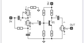
I often see "+" connected intersections in pedal schematics as opposed to "T". Not a big deal to me if I can see the connection easily. Some people loose their poopy if they see an arc where lines cross (see schematic below), doesn't bother me.


What I've learned is mainly that everyone who draws a schematic has their own way of doing it.
Here's one way to draw a simple two transistor fuzz, for instance:
FNJWWOHGPBDGK20.jpg


🙀😹


REALLY? I'd rather look at a sloppy hand-drawn schematic that follows L-R & top-to-bottom flow (inputs left, outputs right) than burn my retinas with the above... At first glance it is legible and clear but... Has the person who drew it ever seen another schematic? A lot of what I've learned is just from looking at LOTS of schematics — most have a standard orientation and flow, and as a budding circuit builder I copy the common standard practices of what I see.

I've seen a circuit where one of the gain stages was inverted, took me a while to realise it, something was off/weird — once I figured out one gain stage was flipped I recognised it was Just Another Muff.

More 101 I've collected:
Resistor values should use the correct suffix (K not k), tolerance should be handled in notes, “e.g. all resistors 1/4W 5% unless noted otherwise”, and the “noted” should be another note.


SPECS: Capacitors, inductors, and resistors get specs instead of part numbers, BUT…
PART #s: Diodes, chips, fuses, oscillators, etc get actual part numbers.
BOM: include a bill of materials that contains all of the information (quantity, designator, manufacturer, part number, description, and other notes) for each and every component on the schematic. So the schematics show only the designator (C1, R45, L2) and the value (0.1uF, 47K, 680uH) for simple parts.

REFERENCE DESCRIPTIONS (ref des) and values go near the part and not near other parts. Be consistent, ex: if the horizontal resistors have ref des above and value below make sure ALL horizontal resistors have ref des above and value below.

'M' and 'm', have entirely different meanings: Big "M" is Mega- and little "m" is milli.
Convention is that positive exponents are uppercase and negative exponents are lowercase, so 'M' is always Mega and 'm' is always milli.
'm' is also the unit for meters
Technically the metric prefix for "kilo" is lowercase "k".
Uppercase "K" is the unit for Kelvins.


LESTRAVELED: I have compared schematic drawing to public speaking. You are communicating to others through the schematic. The schematic is not just a bunch of connections, it is a series of statements that communicate function and intent. Make each sub-schematic a clear statement or function. A badly drawn schematic makes the reader struggle to understand it. A well drawn schematic is understood in seconds.

A schematic is a language, learn to speak it well and everyone will listen. Do it poorly and you will speak to an empty room.


Sorry, don't have links for all the above sources of info.


BEARS REPEATING
🐻🐻🐻🐻🐻🐻🐻🐼🐼🐼🐼🐼🐻🐻🐻🐻🐨🐨🐨🐨🐻🐻🐻🐻‍:
Good schematics show you the circuit. Bad schematics make you decipher them.

So while I've toyed with some schematic concepts such as having all resistors and caps lay horizontally (really weird, really wide),
I generally just try to make my schematics as simple and clean-looking as possible.

C L A R I T Y
 
Last edited:
Well done!
When I would prepare Design Review materials, I always strove to present a clear story that lead the reviewers to the conclusion that I knew what I was doing and the design was solid. If I made the reviewers work too hard to reach that conclusion, my reward was action items.

I'm surprised I haven't run up against the 10K word limit on these forum.
 
Back
Top