Chuck D. Bones
Circuit Wizard
There were some questions in another forum on this site about how to model the analog behavior of the CD4049 and CD4007 in SPICE. I used LTSpice to model my CMOS Distortion pedals, so I thought I'd share that here. To keep things simple, we'll look at the last two stages in the CMOS OD Deluxe. The way to accomplish a resonably accurate simulation of a CMOS inverter in the linear region is to model it at the transistor level. The CMOS inverters in the 4007 (or 4049) each consist of a pair of MOSFETs, one P-channel and one N-channel. M3 and M4 form one inverter, M5 & M6 form another. They operate in a push-pull fashion. Let's look at the last inverter. R20 provides DC feedback around M5 & M6 and along with C10, they bias M5 and M6 into a linear region where both devices are on. The DC voltage at the stage5 node is near 1/2 Vdd. The DRIVE pot and C8 provide DC feedback for M3 and M4. Normally, at low frequency a CMOS gate draws microamps or less from the VDD rail. However when both MOSFETs are on, the MOSFET current is significantly larger. R23 limits the current thru M5 and M6 to a little less than 1mA (same goes for M3 & M4). There is a sweet spot around Vdd = 4.5V where the gain of the MOSFET pair is maximum. In this circuit, Vdd runs close to 6V which provides a little more headroom without giving up too much gain. R17 provides some extra asymmetry and raises the output impedance of stage4. It makes the behavior of the circuit more "tube-like." I set up the signal generator, Vin, to provide a decaying 250Hz sinewave. The peak amplitude is 3Vp-p. This is representative of the output from the previous stage. Rdrive1 and Rdrive2 model the DRIVE pot. Notice the formula for the resistance of Rdrive1. It includes the 68K resistance of R18. I could have drawn in R18 separately, but doing it this way is more compact. I did a similar thing with Rdrive2.

First, we'll run a time-domain (.tran) simulation with D (DRIVE) set to zero. This is the plot of the voltage at stage5. I also plotted Vdd. Notice how Vdd rises slightly at the beginning and settles back as the waveform decays. That's because when the waveform is at it's peaks, one of the MOSFETs in a pair is turned off and the Vdd current drops. C16 limits how far and how fast Vdd can change.

Same plot with D = 1 (max DRIVE).
Notice how the initial decay levels off around 160ms and then resumes around 200ms. The envelope shape is partly due to the Vdd sag and partly to the 5th stage loading the 4th stage. It's a natural "breathing" effect similar to amplifier sag.
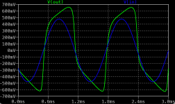
When we zoom in, we can see how the waveshape changes.


We can also run an AC plot to see how the freq response changes when we change DRIVE.

C11 and R20 roll-off the top end pretty strongly. Some of the top end can be recovered by advancing the TREBLE control.
That's about it.

First, we'll run a time-domain (.tran) simulation with D (DRIVE) set to zero. This is the plot of the voltage at stage5. I also plotted Vdd. Notice how Vdd rises slightly at the beginning and settles back as the waveform decays. That's because when the waveform is at it's peaks, one of the MOSFETs in a pair is turned off and the Vdd current drops. C16 limits how far and how fast Vdd can change.

Same plot with D = 1 (max DRIVE).

Notice how the initial decay levels off around 160ms and then resumes around 200ms. The envelope shape is partly due to the Vdd sag and partly to the 5th stage loading the 4th stage. It's a natural "breathing" effect similar to amplifier sag.
When we zoom in, we can see how the waveshape changes.


We can also run an AC plot to see how the freq response changes when we change DRIVE.

C11 and R20 roll-off the top end pretty strongly. Some of the top end can be recovered by advancing the TREBLE control.
That's about it.