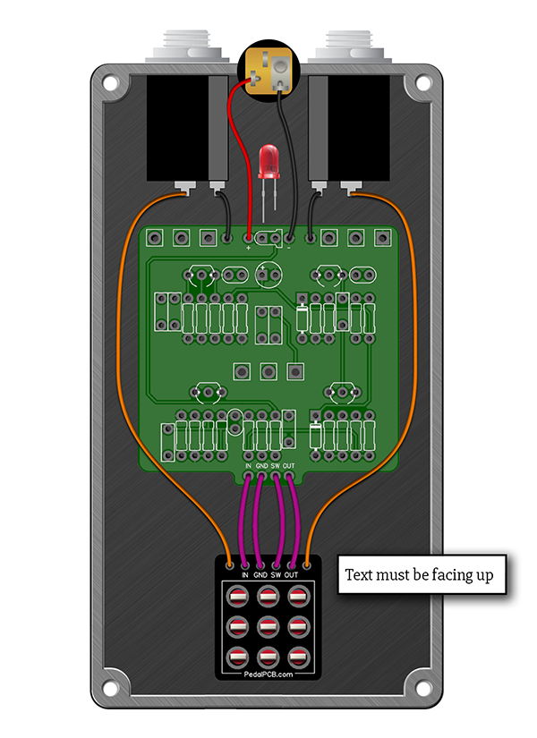
The fun never ends. I just finished drilling all the holes and mounting the hardware, so all that remains is to wire it up, and that's when I came to a dead halt.
For clarity, this appears to be a Rev 1 board, due to the components and layout, plus the switches are closer together compared with the newer drill template.
Here we go:
At the top of the board, nearest the power jack and in/out jacks (all top mounted as per the template), there are four holes, all with no label.
At the bottom of the board, nearest the stomp switch are four more holes.
On the SB wiring diagram, there are six holes at the top and four at the bottom, all labeled.
Since nothing was labeled, I hate to assume, so I put the meter on continuity and found the following:
Let's call the holes 1-4 starting from left to right.
At the top of the board, holes 1 and 2 are together, and are connected to hole 3 at the bottom. My guess is that one of the two holes at the top receives power from the jack and the other provides power to the onboard CLR, sheer guess.
At the top of the board, hole 3 does not appear to connect to anything, but hole 4 also connects to hole 3 at the bottom.
It would REALLY be helpful to obtain a schematic (page 4), wiring diagram (page 5), and component value pictorial (page 2) for the Rev 1 board I actually have. Newer versions just don't appear to be close enough to generalize.
I am not the world's greatest visualizer so as I often do, I picked too small an enclosure, so everything is a tight fit. I suppose, if I have to, I can remove the board from the enclosure and trace the wiring manually, but I am hoping I am not the only one who found themselves in this boat.
Also, I got conflicting advice about the output resistor R13. On the schematic I have, it shows a 10 ohm resistor. On the board, it shows 100K - quite a difference. One person on the forum told me to use the value on the board (100K) and another told me to disregard that and use 10 ohms, which I did. That much difference should certainly make a huge difference in the amplitude of the output, so does anyone know which value I should be using?
Finally, I had intended to use one of those large blue stomp switches, which I have way too many of, since it has the built-in LED, but it is too big to fit, so I have gone back to a regular-size switch. Normally, I would use the PPCD daughter board, but I only have one left (I already soldered my second-to-last one to the big blue switch) and don't want to use it if there is no 1-1 relationship between it's holes and the ones on the board.
If I use another outfit's daughter board, I can more easily wire up the input and output jacks, plus it makes it a LOT easier to wire up an LED near the switch. I have NO idea where to put an LED if I can't do it that way.
In my own defense, I didn't buy this board directly from PPCB. I ran into a guy on Reddit who said he had ADHD and was getting out of building pedals. I bought a ton of stuff from him, and this board was part of that.
Okay, I will shut up now and hope for some very much appreciated assistance. Thanks in advance. I suppose this is what I get for using an out of date board.
Bud


