debrad
Active member
Hi PedalPCB friends!
I'm aiming to make a modification to a NON-PedalPCB circuit but I thought I'd check in here...a) to solicit your wisdom and b) to share the discussion with those of you who may grapple with a similar situation down the road.
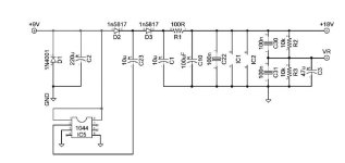
As shown in the schematic below, the board has a charge pump to boost the 9v input to 18v but the fellow I'm building for wants to run it directly off an 18v input so in my attempt to bypass the charge pump, I'm hoping to get some advice on the components in the power section.

Based on my limited knowledge, it appears that D1 (1N4001) and C2 (220uf electrolytic) form a parallel reverse polarity protection while D2 and D3 (1N5817) form series reverse polarity protection for the 9v input (D2) and the charge pump's 18v output (D3) respectively.
After speaking with the circuit designer, I am still not 100% sure if I should:
Can someone please confirm or correct my understanding of this part of the power input and/or provide me with some advice on the best way to proceed with this particular modification?
Thanks so much!
- brad -
I'm aiming to make a modification to a NON-PedalPCB circuit but I thought I'd check in here...a) to solicit your wisdom and b) to share the discussion with those of you who may grapple with a similar situation down the road.
As shown in the schematic below, the board has a charge pump to boost the 9v input to 18v but the fellow I'm building for wants to run it directly off an 18v input so in my attempt to bypass the charge pump, I'm hoping to get some advice on the components in the power section.

Based on my limited knowledge, it appears that D1 (1N4001) and C2 (220uf electrolytic) form a parallel reverse polarity protection while D2 and D3 (1N5817) form series reverse polarity protection for the 9v input (D2) and the charge pump's 18v output (D3) respectively.
After speaking with the circuit designer, I am still not 100% sure if I should:
- omit D1 + C2 and jumper D2 to leave myself with D3 as the only series reverse polarity protection,
- install D1, C2, and D3 with a jumper replacing D2, or
- do something else entirely.
Can someone please confirm or correct my understanding of this part of the power input and/or provide me with some advice on the best way to proceed with this particular modification?
Thanks so much!
- brad -
Last edited:

