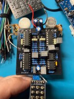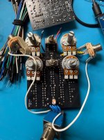

LFO does not oscillate. The phaser effect works manually (turning pots changes the tone), but nothing sweeps. Board is out of the enclosure for inspection. All ICs are socketed.
I take super detailed troubleshooting notes so hopefully someone can see something in here and call out my mistake!
## What I've Already Ruled Out
**All three LFO ICs eliminated via swapping:**
- Swapped IC4 and IC5 (TL072s in the LFO section) with known good TL072s. No change.
- Swapped IC3 (LM13700, LFO OTA) with IC1 (a known working LM13700 from the phase shift section). No change.
**Power rails confirmed on every IC:**
| IC | Part | V+ Reading | V- Reading |
|----|------|-----------|-----------|
| IC1 | LM13700 | 8.85V | 0V |
| IC2 | LM13700 | 8.85V | 0V |
| IC3 | LM13700 | 8.85V | 0V |
| IC4 | TL072 | 8.86V | 0V |
| IC5 | TL072 | 8.85V | 0V |
All clean.
## Scope Confirms Dead LFO
Probed all four TL072 LFO outputs (1V/div, 500ms/div, DC coupling, no input signal):
| Probe Point | Result |
|------------|--------|
| IC4 Pin 1 | Flat line, noise only at 10mV/div |
| IC4 Pin 7 | Flat line |
| IC5 Pin 1 | Flat line |
| IC5 Pin 7 | Flat line |
No oscillation on any output.
## Voltage Dumps
### IC3 (LM13700, LFO OTA)
| Pin | Function | DC Voltage | Notes |
|-----|----------|-----------|-------|
| 1 | IABC1 (bias input) | ~1.05V | Responds to Rate pot |
| 2 | Diode bias 1 | 0V | |
| 3 | Inverting input 1 | 5.78V | Higher than expected |
| 4 | Non-inv input 1 | Drifts 4V → 1.18V | Charges one direction then stalls |
| 5 | Output 1 | 0.33V | Nearly railed low |
| 6 | V- | 0V | |
| 7 | Darlington base 1 | ~0.36V (jumpy) | |
| 8 | Darlington emitter 1 | 1.18V | |
| 9 | Darlington emitter 2 | 0.92V | |
| 10 | Darlington base 2 | 0.92V | |
| 11 | V+ | 8.85V | |
| 12 | Output 2 | 0.92V | Jittery on scope |
| 13 | Non-inv input 2 | 1.18V | Low, expected ~4.4V |
| 14 | Inv input 2 | 0.06V | Nearly ground |
| 15 | Diode bias 2 | 0V | |
| 16 | IABC2 (bias input) | ~1.2V | |
**Key finding on Pin 4:** Voltage starts around 4V then drifts down to 1.18V and stalls. Looks like the integrator cap charges one direction but never gets the trigger to reverse.
**Pins 13 and 14** are both well below expected half supply (~4.4V). Section 2 of the OTA may not be functioning as the comparator correctly.
### IC4 (TL072, LFO)
| Pin | Function | DC Voltage |
|-----|----------|-----------|
| 1 | Output A | 4.42V |
| 2 | Inv input A | 4.42V |
| 3 | Non-inv input A | 4.30V |
| 4 | V- | 0V |
| 5 | Non-inv input B | 4.42V |
| 6 | Inv input B | 4.42V |
| 7 | Output B | 4.42V |
| 8 | V+ | 8.85V |
All at half supply. Healthy but idle.
### IC5 (TL072, LFO)
| Pin | Function | DC Voltage |
|-----|----------|-----------|
| 1 | Output A | 4.42V |
| 2 | Inv input A | 4.42V |
| 3 | Non-inv input A | **2.21V** | Only pin not at half supply |
| 4 | V- | 0V |
| 5 | Non-inv input B | 4.42V |
| 6 | Inv input B | 4.42V |
| 7 | Output B | 4.42V |
| 8 | V+ | 8.85V |
IC5 Pin 3 is the outlier at 2.21V (exactly half of the 4.42V half supply). Measured ~97K to ground on the 200K range at that node. R3 is 1M to the bias network on one side. Something is pulling that pin lower than it should be.
## My Theory
Since all ICs are ruled out, the problem is a passive component or trace in the LFO feedback loop between IC3 and IC5. The integrator (IC3 pin 4) charging one way and stalling suggests the feedback path that triggers reversal is broken.
## What I've Already Checked / Ruled Out
- **RANGE toggle position:** Confirmed NOT in the middle (off) position. Tested both throw positions.
- **All ICs swapped** with known good chips. No change.
- **Power rails clean** on all 5 ICs.
- **IC5 pin 3 at 2.21V:** I now understand this is **normal** (half of Vref via R3 1M divider, not a fault).
## What I'm Checking Next
Based on research, here's my priority list. Posting this in case someone can save me time by spotting the problem from the voltage dumps above:
**1. Resistor values in the LFO loop (pulling and measuring each):**
| Ref | Should Be | Common Misread | What It Does |
|-----|-----------|---------------|-------------|
| R28 | 220K | 220R (missing orange band) | Integrator gain |
| R29 | 100K | 100R or 1M | Integrator feedback |
| R30 | 150K | 15K or 1M5 | Schmitt trigger threshold |
| R31 | 10K | 1K or 100K | Schmitt trigger hysteresis |
| R32 | 4K7 | 470R or 47K | OTA bias |
| R33 | 4K7 | 470R or 47K | OTA bias |
| R34 | 470K | 47K or 4K7 | Max RATE range |
**2. C13 (1µF) and C14 (4µ7) timing caps:** Verifying correct value, polarity, and checking for leakage. I've seen reports of 1nF (102 marking) being mistaken for 1µF (105).
**3. Chuck D. Bones mods #8 and #9:** Adding 3.3MΩ from RATE pot pin 3 to Vref, and 22KΩ from IC3 pin 8 to GND. He calls these mandatory for reliable LFO startup. Planning to add these if resistor/cap verification doesn't solve it.
**4. Continuity check** on the feedback path from IC5 pin 1 through R28/R29 and from IC5 pin 7 back through the OTA loop.
## What I Need Help With
If anyone has a working Circulator and can share voltage readings at IC3 pins 3, 4, 5, and IC5 pins 1, 6, 7 for comparison, that would help narrow things down. Or if the voltage dumps above scream "wrong resistor at Rxx" to anyone who knows this circuit well, I'm all ears.
Also, has anyone done the Chuck D. Bones mods #8 and #9 and can confirm they solved a similar stall issue?
Thanks for any help!
I'll post some pictures here in a few!
I take super detailed troubleshooting notes so hopefully someone can see something in here and call out my mistake!
## What I've Already Ruled Out
**All three LFO ICs eliminated via swapping:**
- Swapped IC4 and IC5 (TL072s in the LFO section) with known good TL072s. No change.
- Swapped IC3 (LM13700, LFO OTA) with IC1 (a known working LM13700 from the phase shift section). No change.
**Power rails confirmed on every IC:**
| IC | Part | V+ Reading | V- Reading |
|----|------|-----------|-----------|
| IC1 | LM13700 | 8.85V | 0V |
| IC2 | LM13700 | 8.85V | 0V |
| IC3 | LM13700 | 8.85V | 0V |
| IC4 | TL072 | 8.86V | 0V |
| IC5 | TL072 | 8.85V | 0V |
All clean.
## Scope Confirms Dead LFO
Probed all four TL072 LFO outputs (1V/div, 500ms/div, DC coupling, no input signal):
| Probe Point | Result |
|------------|--------|
| IC4 Pin 1 | Flat line, noise only at 10mV/div |
| IC4 Pin 7 | Flat line |
| IC5 Pin 1 | Flat line |
| IC5 Pin 7 | Flat line |
No oscillation on any output.
## Voltage Dumps
### IC3 (LM13700, LFO OTA)
| Pin | Function | DC Voltage | Notes |
|-----|----------|-----------|-------|
| 1 | IABC1 (bias input) | ~1.05V | Responds to Rate pot
|| 2 | Diode bias 1 | 0V | |
| 3 | Inverting input 1 | 5.78V | Higher than expected |
| 4 | Non-inv input 1 | Drifts 4V → 1.18V |
Charges one direction then stalls || 5 | Output 1 | 0.33V | Nearly railed low |
| 6 | V- | 0V |
|| 7 | Darlington base 1 | ~0.36V (jumpy) | |
| 8 | Darlington emitter 1 | 1.18V | |
| 9 | Darlington emitter 2 | 0.92V | |
| 10 | Darlington base 2 | 0.92V | |
| 11 | V+ | 8.85V |
|| 12 | Output 2 | 0.92V | Jittery on scope |
| 13 | Non-inv input 2 | 1.18V |
Low, expected ~4.4V || 14 | Inv input 2 | 0.06V |
Nearly ground || 15 | Diode bias 2 | 0V | |
| 16 | IABC2 (bias input) | ~1.2V | |
**Key finding on Pin 4:** Voltage starts around 4V then drifts down to 1.18V and stalls. Looks like the integrator cap charges one direction but never gets the trigger to reverse.
**Pins 13 and 14** are both well below expected half supply (~4.4V). Section 2 of the OTA may not be functioning as the comparator correctly.
### IC4 (TL072, LFO)
| Pin | Function | DC Voltage |
|-----|----------|-----------|
| 1 | Output A | 4.42V |
| 2 | Inv input A | 4.42V |
| 3 | Non-inv input A | 4.30V |
| 4 | V- | 0V |
| 5 | Non-inv input B | 4.42V |
| 6 | Inv input B | 4.42V |
| 7 | Output B | 4.42V |
| 8 | V+ | 8.85V |
All at half supply. Healthy but idle.
### IC5 (TL072, LFO)
| Pin | Function | DC Voltage |
|-----|----------|-----------|
| 1 | Output A | 4.42V |
| 2 | Inv input A | 4.42V |
| 3 | Non-inv input A | **2.21V** |
Only pin not at half supply || 4 | V- | 0V |
| 5 | Non-inv input B | 4.42V |
| 6 | Inv input B | 4.42V |
| 7 | Output B | 4.42V |
| 8 | V+ | 8.85V |
IC5 Pin 3 is the outlier at 2.21V (exactly half of the 4.42V half supply). Measured ~97K to ground on the 200K range at that node. R3 is 1M to the bias network on one side. Something is pulling that pin lower than it should be.
## My Theory
Since all ICs are ruled out, the problem is a passive component or trace in the LFO feedback loop between IC3 and IC5. The integrator (IC3 pin 4) charging one way and stalling suggests the feedback path that triggers reversal is broken.
## What I've Already Checked / Ruled Out
- **RANGE toggle position:** Confirmed NOT in the middle (off) position. Tested both throw positions.
- **All ICs swapped** with known good chips. No change.
- **Power rails clean** on all 5 ICs.
- **IC5 pin 3 at 2.21V:** I now understand this is **normal** (half of Vref via R3 1M divider, not a fault).
## What I'm Checking Next
Based on research, here's my priority list. Posting this in case someone can save me time by spotting the problem from the voltage dumps above:
**1. Resistor values in the LFO loop (pulling and measuring each):**
| Ref | Should Be | Common Misread | What It Does |
|-----|-----------|---------------|-------------|
| R28 | 220K | 220R (missing orange band) | Integrator gain |
| R29 | 100K | 100R or 1M | Integrator feedback |
| R30 | 150K | 15K or 1M5 | Schmitt trigger threshold |
| R31 | 10K | 1K or 100K | Schmitt trigger hysteresis |
| R32 | 4K7 | 470R or 47K | OTA bias |
| R33 | 4K7 | 470R or 47K | OTA bias |
| R34 | 470K | 47K or 4K7 | Max RATE range |
**2. C13 (1µF) and C14 (4µ7) timing caps:** Verifying correct value, polarity, and checking for leakage. I've seen reports of 1nF (102 marking) being mistaken for 1µF (105).
**3. Chuck D. Bones mods #8 and #9:** Adding 3.3MΩ from RATE pot pin 3 to Vref, and 22KΩ from IC3 pin 8 to GND. He calls these mandatory for reliable LFO startup. Planning to add these if resistor/cap verification doesn't solve it.
**4. Continuity check** on the feedback path from IC5 pin 1 through R28/R29 and from IC5 pin 7 back through the OTA loop.
## What I Need Help With
If anyone has a working Circulator and can share voltage readings at IC3 pins 3, 4, 5, and IC5 pins 1, 6, 7 for comparison, that would help narrow things down. Or if the voltage dumps above scream "wrong resistor at Rxx" to anyone who knows this circuit well, I'm all ears.
Also, has anyone done the Chuck D. Bones mods #8 and #9 and can confirm they solved a similar stall issue?
Thanks for any help!
I'll post some pictures here in a few!