How many times do we see post in the Troubleshooting forum where the problem turns out to be a JFET?
Like Germanium transistors, JFETs are finicky beasts and buying the right part number does not guarantee success.
First, a very brief primer on how JFETs work.
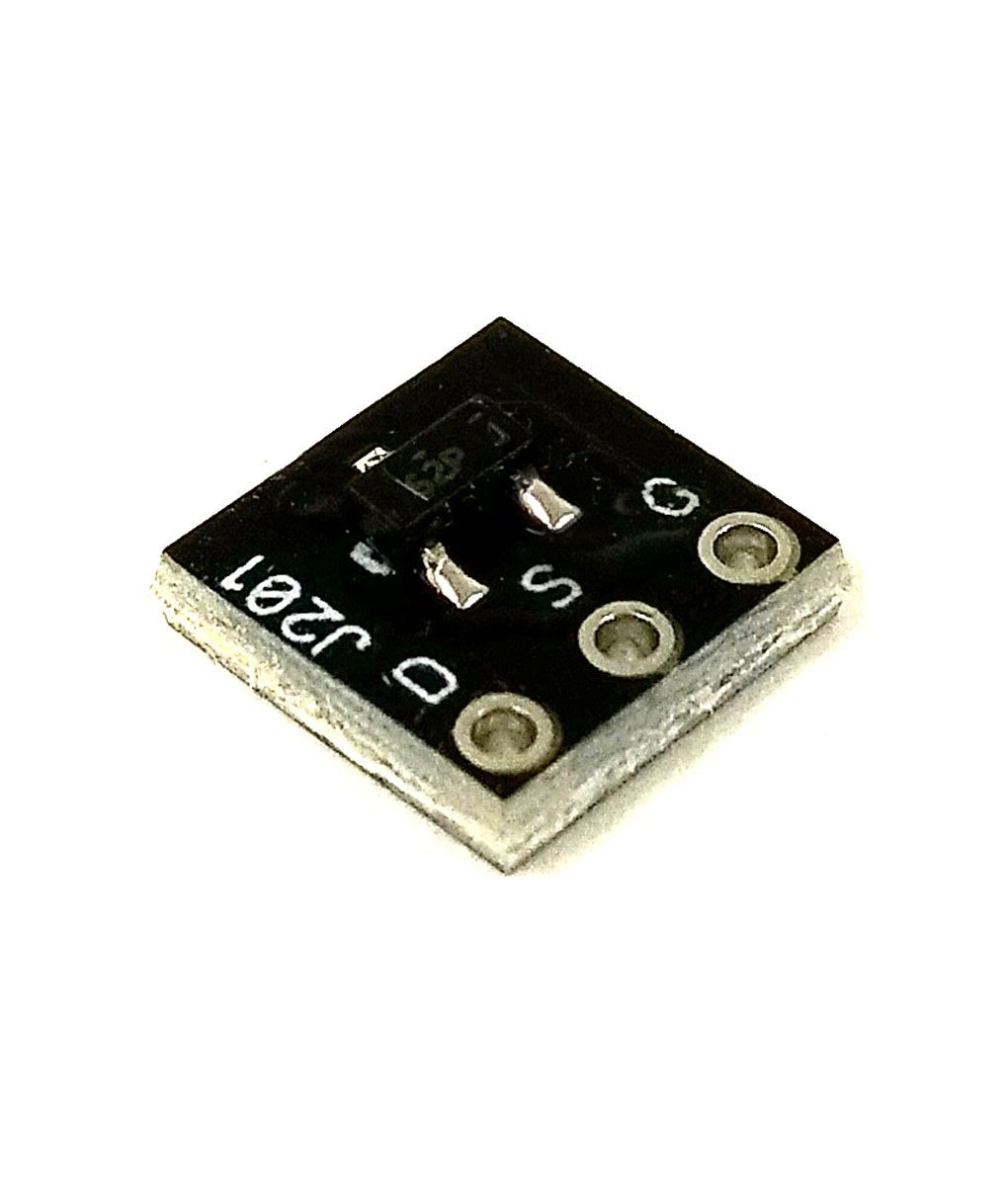
JFETs are voltage-controlled devices. The drain current depends on Vgs (the voltage between gate & source). The gate current is so close to zero that we can safely assume it is zero. We'll talk about N-channel JFETs (arrow on the gate pointing in) because 99% of the time that's what are used in pedals. When Vgs is zero, the JFET is fully on; the drain current is Idss. When we make Vgs go negative, the drain current is reduced. When Vgs reaches Vp, the drain current is zero. When we using JFETs to amplify signals, Vgs will be somewhere between 0 and Vp.
JFET specs
The two JFET specs we care about are Vp and Idss. Those two number tell the pedal circuit designer all they need to know to set the bias and determine the gain of the JFET. Here's where it gets ugly. The Vp and Idss specs on JFETs are extremely loose. Some more than others. Example: 2N5457 has a Vp spec from 0.5V to 6.0V. The Idss spec is 1mA to 5mA. Parts at the extreme end of those ranges will probably not work in a given pedal. As good as JFET production methods are, there is still a significant variation from lot-to-lot. The manufacturers test and sort the JFETs, but to keep yields up and costs down, the specs are left pretty loose. It is very common for OEMs (Original Equipment Manufacturers), to either pay the JFET manufacturers to cherry-pick JFETs to fit a narrower spec window, or buy lots of extras and do it themselves. We're in the position where we have to do it ourselves. Sometimes, the pedal designer is clever enough to design a circuit that can tolerate the variations in Vp or Idss. Of all the JFET pedals sold on this site, only a few fall into that category. That's why JFET pedals have trimmers in them. But the trimmer can only do so much and a JFET that is near the extremes for Vp or Idss may not work for any trimmer setting.
Why do pedal designers use JFETs if they're so problematic?
JFETs have certain advantages. In some circuits, they can have more gain and/or less noise than bipolar transistors. Their input impedance is very large, so they don't load down pickups or other stages in the pedal. Their biggest appeal to pedal builders is that their transfer function is similar to that of a vacuum tube. They tend to generate lower-order harmonics and overload more gracefully in a properly designed circuit, compared to bipolar transistors. Many of the amp-in-a-box pedals replicate a tube amp's preamp section, with JFETs standing in for vacuum tubes.
What do we do about it?
Well, first you go to college for four years and get a degree in electrical engineering. Ok, so that's not going to work for most people. The alternatives are you find someone who can analyze the circuit and recommend a range for Vp and Idss, or you find someone who has measured a production pedal and try to match their readings. Luckily, there are forums inside and outside this website that can help you with that. Mr. PedalPCB might be persuaded to include JFET spec requirements in the Build Docs for pedals that are picky about such things. You need to own and understand how to use a transistor tester. You can get a perfectly adequate one for about $20US on eBay. The other thing you need to do is you buy quality parts from a reputable vendor*. I've said it before and it bears repeating here: "If you buy transistors on eBay, you need to have the heart of a gambler and the skill to test them." If there was ever a place that demonstrates the adage "If it's too good to be true, it probably is." it's eBay. There are some good semiconductor vendors on eBay, but they are in the minority. The rest are either ignorant or crooks because there are a TON of counterfeit parts sold there.
* A high score on eBay does not a "reputable vendor" make. They might have earned that high score selling umbrellas.
The Bottom Line
Building pedals containing JFETs is not necessarily a paint-by-numbers activity and you need to know that going in. Unless you screen your JFETs prior to assembly, sockets are mandatory. Buy from a reputable vendor and buy at least 3x as many as you will need so you end up with enough that work in your pedal.
Next Time: Biasing JFETs
Like Germanium transistors, JFETs are finicky beasts and buying the right part number does not guarantee success.
First, a very brief primer on how JFETs work.
JFETs are voltage-controlled devices. The drain current depends on Vgs (the voltage between gate & source). The gate current is so close to zero that we can safely assume it is zero. We'll talk about N-channel JFETs (arrow on the gate pointing in) because 99% of the time that's what are used in pedals. When Vgs is zero, the JFET is fully on; the drain current is Idss. When we make Vgs go negative, the drain current is reduced. When Vgs reaches Vp, the drain current is zero. When we using JFETs to amplify signals, Vgs will be somewhere between 0 and Vp.
JFET specs
The two JFET specs we care about are Vp and Idss. Those two number tell the pedal circuit designer all they need to know to set the bias and determine the gain of the JFET. Here's where it gets ugly. The Vp and Idss specs on JFETs are extremely loose. Some more than others. Example: 2N5457 has a Vp spec from 0.5V to 6.0V. The Idss spec is 1mA to 5mA. Parts at the extreme end of those ranges will probably not work in a given pedal. As good as JFET production methods are, there is still a significant variation from lot-to-lot. The manufacturers test and sort the JFETs, but to keep yields up and costs down, the specs are left pretty loose. It is very common for OEMs (Original Equipment Manufacturers), to either pay the JFET manufacturers to cherry-pick JFETs to fit a narrower spec window, or buy lots of extras and do it themselves. We're in the position where we have to do it ourselves. Sometimes, the pedal designer is clever enough to design a circuit that can tolerate the variations in Vp or Idss. Of all the JFET pedals sold on this site, only a few fall into that category. That's why JFET pedals have trimmers in them. But the trimmer can only do so much and a JFET that is near the extremes for Vp or Idss may not work for any trimmer setting.
Why do pedal designers use JFETs if they're so problematic?
JFETs have certain advantages. In some circuits, they can have more gain and/or less noise than bipolar transistors. Their input impedance is very large, so they don't load down pickups or other stages in the pedal. Their biggest appeal to pedal builders is that their transfer function is similar to that of a vacuum tube. They tend to generate lower-order harmonics and overload more gracefully in a properly designed circuit, compared to bipolar transistors. Many of the amp-in-a-box pedals replicate a tube amp's preamp section, with JFETs standing in for vacuum tubes.
What do we do about it?
Well, first you go to college for four years and get a degree in electrical engineering. Ok, so that's not going to work for most people. The alternatives are you find someone who can analyze the circuit and recommend a range for Vp and Idss, or you find someone who has measured a production pedal and try to match their readings. Luckily, there are forums inside and outside this website that can help you with that. Mr. PedalPCB might be persuaded to include JFET spec requirements in the Build Docs for pedals that are picky about such things. You need to own and understand how to use a transistor tester. You can get a perfectly adequate one for about $20US on eBay. The other thing you need to do is you buy quality parts from a reputable vendor*. I've said it before and it bears repeating here: "If you buy transistors on eBay, you need to have the heart of a gambler and the skill to test them." If there was ever a place that demonstrates the adage "If it's too good to be true, it probably is." it's eBay. There are some good semiconductor vendors on eBay, but they are in the minority. The rest are either ignorant or crooks because there are a TON of counterfeit parts sold there.
* A high score on eBay does not a "reputable vendor" make. They might have earned that high score selling umbrellas.
The Bottom Line
Building pedals containing JFETs is not necessarily a paint-by-numbers activity and you need to know that going in. Unless you screen your JFETs prior to assembly, sockets are mandatory. Buy from a reputable vendor and buy at least 3x as many as you will need so you end up with enough that work in your pedal.
Next Time: Biasing JFETs