- Build Rating
- 5.00 star(s)
It works! See here for the background: Plug-n-Play Buffered Electrical Bypass Using CD4053 and Momentary SPST.
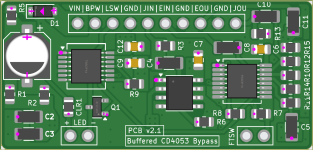
In short, it's a dedicated circuit and PCB that does two things: (1) always-on buffer, and (2) electrical bypass via CD4053. This is essentially how Boss pedals do buffering and bypass, but with integrated circuits (instead of discrete).
The actual effect is yet another revision on @Chuck D. Bones's great modified Animals Diamond Peak circuit. This is the third revision, which was mostly purpose-built for testing this bypass module. (First board build report, Second board revision build report) In this latest (third) revision, besides dropping the integrated relay bypass circuitry, I also opted for using a BJT instead of a JFET for Q1. This was done mostly out of curiosity.
Eagle-eyed viewers will note my nasty solder job on transistors Q2 and Q3. These are the "money" transistors you can roll to tweak the tone. I initially used the same transistors I used in a previous build, just to reduce the number of variables. Once I verified it was working, I swapped transistors because I wanted to try something different. That turned into a huge debacle - I nearly destroyed the solder pads removing the original transistors. Normally I'm pretty good at cleanly replacing components, so I don't know what happened here. It took a couple touch-ups with the soldering iron to actually make the circuit work with the new transistors.
I actually stole the enclosure from the most recent build (second board revision).
But the excitement here is the bypass board. I had help from the folks at DIYstompboxes on the circuit.
Repeating part of my previous post, my goals here are:
I haven't measured power consumption yet, but unless I made a mistake, it should be very battery-friendly.
The only real downside here is the physical size, but the next step is to have SMD versions prebuilt; the SMD version design is almost done, and it's dramatically smaller (currently 22x45mm). I wanted the prototype to be through-hole in case I had to debug. The other obvious downside to a design like this (as with Boss pedals), even bypass requires power, so the circuit is completely worthless without power. But the same goes for my amp.")
I have plenty of extra bypass boards, happy to give them away for free, just PM me. I also have a few extra Diamond Peak boards available (both this and previous versions), also free, just drop me a PM.
In short, it's a dedicated circuit and PCB that does two things: (1) always-on buffer, and (2) electrical bypass via CD4053. This is essentially how Boss pedals do buffering and bypass, but with integrated circuits (instead of discrete).
The actual effect is yet another revision on @Chuck D. Bones's great modified Animals Diamond Peak circuit. This is the third revision, which was mostly purpose-built for testing this bypass module. (First board build report, Second board revision build report) In this latest (third) revision, besides dropping the integrated relay bypass circuitry, I also opted for using a BJT instead of a JFET for Q1. This was done mostly out of curiosity.
Eagle-eyed viewers will note my nasty solder job on transistors Q2 and Q3. These are the "money" transistors you can roll to tweak the tone. I initially used the same transistors I used in a previous build, just to reduce the number of variables. Once I verified it was working, I swapped transistors because I wanted to try something different. That turned into a huge debacle - I nearly destroyed the solder pads removing the original transistors. Normally I'm pretty good at cleanly replacing components, so I don't know what happened here. It took a couple touch-ups with the soldering iron to actually make the circuit work with the new transistors.
I actually stole the enclosure from the most recent build (second board revision).
But the excitement here is the bypass board. I had help from the folks at DIYstompboxes on the circuit.
Repeating part of my previous post, my goals here are:
- Transparent buffer
- No mechanical parts to wear out (this doesn't include the momentary SPST, which is only two wires and easily replaced)
- Ultra-low power consumption
- Low cost
- Use modern, readily-available commodity parts.
I haven't measured power consumption yet, but unless I made a mistake, it should be very battery-friendly.
The only real downside here is the physical size, but the next step is to have SMD versions prebuilt; the SMD version design is almost done, and it's dramatically smaller (currently 22x45mm). I wanted the prototype to be through-hole in case I had to debug. The other obvious downside to a design like this (as with Boss pedals), even bypass requires power, so the circuit is completely worthless without power. But the same goes for my amp.
I have plenty of extra bypass boards, happy to give them away for free, just PM me. I also have a few extra Diamond Peak boards available (both this and previous versions), also free, just drop me a PM.


") But not for e.g. EffectsLayouts, Aion, Madbean, etc.
But not for e.g. EffectsLayouts, Aion, Madbean, etc.