You are using an out of date browser. It may not display this or other websites correctly.
You should upgrade or use an alternative browser.
You should upgrade or use an alternative browser.
Lt1054 negative voltage grounds
- Thread starter rossbalch
- Start date
Mcknib
Well-known member
I've never used separate grounds for voltage converter circuits
I think it's maybe just a personal indicator to separate the parts used to convert the voltage you'll notice it starts at the charge pump protection zener
Certainly the datasheets don't specify using separate grounds
I think it's maybe just a personal indicator to separate the parts used to convert the voltage you'll notice it starts at the charge pump protection zener
Certainly the datasheets don't specify using separate grounds
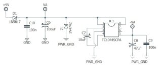
In your example I'm guessing PWR_GND is a separate ground pour around the charge pump to help isolate the switching noise and prevent it from coupling into the audio signal. Power ground and signal ground then likely meet only at a single point somewhere around the main filtering capacitors C6/C10. This probably won't matter on a breadboard though which is inherently noisy, so I wouldn't worry about it.
Mcknib
Well-known member
From Kevin at Aion you sparked my interest so I asked:
They're separate on the main board, but they connect up on the footswitch board. it's just a way to keep the analog signal as far as possible from the high-frequency oscillation of the charge pump. It's somewhat specific to the way our pedals are designed rather than something that would be seen in the chip's datasheet.
Kevin
drew.spriggs
Well-known member
This is switching power supply PCB design 101 - you tie the separate grounds back at a singular point (preferably the DC jack, or at the bucket cap before the switcher.
Using this schematic from AionFX to build a negative voltage supply for my bread board. I notice they have separate ground for the negative voltage compared to the input filtering. Is this necessary or just to minimise switching noise?
View attachment 100374
Minimising switching noise. Current flows in loops, and that (being high frequency and with higher harmonics) follows the impedance rather than resistance that DC does. This can mean flow through the components rather than the actual PCB ground planes!
Anyone interested may be interested in this article which visually shows the return path over a ground plane changing.
Also this may be an interesting read: https://www.nwengineeringllc.com/article/how-to-design-your-pcb-return-current-path.php
It's worth noting that there will be a high frequency loop from you -VA to the inductor used for the switching (ie pin 3). I'd look at the reference design of the PCB as I would assume the C8 and C9 may be close to the 1044 (C8 almost spanning pin 5 to pin 3) to allow a fast return without making the switching noise find a path of least impedance across the components of the board.
I would also bypass the power on the 'primary side' close to the chip for the same reason. You can use a seperate power plane, but ensure the bypass caps connect to the right plane. It gets more complex with off board connections with multiple power planes.
I did a lot of work around this designing PCBs 24MHz clock and components. Usually, unless you have modelling software capable of modelling the flows themselves, then it's recommended to keep it simple with a thick common ground plane.
I have had seperate ground planes but that was part of a galvanic isolation where each side had their own totally completely separate power and ground to reduce noise.
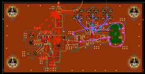
This was me trying to visualise the current paths for low frequency and high frequency. The left has a shunt power supply (a constant current that is super low impedance) and the right has a 24MHz clock, power inductors and decoupling cap filters, the signal goes through a spanning chip and via coaxial ports so the off board power return is shown. This is a 4 layer board and the low noise oscillator can't have copper underneath it hence the hole. Red is DC, then the other paths have both out and return with the same colour. Pink is oscillator power and return, blue is generated signal/span and return.

The resulting clock was extremely low noise and low phase noise. (the mounting via 'gnd' was sat on an isolating standoffs of anyone was wondering)
Last edited:

