z2amiller
Active member
Pitfalls and Tips: Designing effects PCBs
Intro
Following up on my ‘Getting Started with PCBA at JLC’ document, I thought I’d create something similar documenting some of my big mistakes and learnings from creating these PCBs.
This isn’t my job or my background, I’m just doing this for fun and it’s all about learning-by-doing (rather, learning-by-making-mistakes-and-starting-over). But hopefully some of my mistakes (especially my repeated mistakes) can become someone else’s learning.
This isn't a "how to design PCBs" post - there's quite a bit of assumed knowledge here so maybe people who know how to design PCBs in KiCad already know most of this.
Common Mistakes (at least for me)
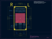
Right vs Left
99% of everyone (sample size: me) will design their pedals with the components on the “front” side of the board (red) and the controls (pots, switches) on the “back” side of the board (blue). But remember that when you’re looking at the front of the board in KiCad, you’re looking at the back of the board when it’s assembled and right-side-up.
That means that the left and right sides of the board are reversed - if you want the volume pot to be on the upper left side of the enclosure, it needs to be in the upper right of the KiCad layout.
Reversed Potentiometers
This can happen both in the schematic and in the PCB layout. Doublecheck that your schematic has the pots turning the right way – some schematics label pin 1 as “CCW”. Some schematics don’t label it at all and you have to figure it out from context. (A much longer discussion). Once you’re laying out, make sure that the pots are on the correct side of the board (probably the back) to make sure that pin1 is in the correct position - for pots on the back side of the board, pin1 will be on the right side in the default KiCad view. This undoes the reversal mentioned above; when flipped over, pin1/CCW is in the correct place on the left.
DC Power Jacks
I kind of hate the weird honkin plastic dongle thingies and even the slim-line DC connectors that seem to be the standard things that people build pedals with. It took me trying and failing with about a half a dozen of the nicer metal ones before it dawned on me that the reason that effects builders use these stupid looking power connectors is that the power standard for pedals is tip-negative, sleeve-positive, and these nice metal jacks connect the sleeve to the metal part, and then therefore the enclosure, and then therefore you short it out because some other thing is grounded to your enclosure but your enclosure is connected to the 9V rail.
Externally-Mounted Hardware
This is kind of obvious once you have it in your hands, but when it’s just a CAD rendering you might not realize it. You can only have things sticking out of one ‘face’ of your enclosure and still be able to easily assemble it. Otherwise you’ll probably have to drill out some of the holes to a large diameter, or you’ll have to install it partially assembled and solder the jacks on in-situ. There are a couple of ways around this, see ‘Daughterboards’ and ‘One Piece Boards’.
KiCad’s Default TO-92 Through Hole Transistor Footprints Kinda Suck

The holes are really close together and sometimes not enough soldermask gets between them. Then you end up soldering the pins of your transistors together. There are footprints called TO92_Inline_Wide that have the leads set further apart.
PCBA: Doublecheck Your BOM
If you’re getting JLC PCBA, doublecheck your BOM at the BOM review step.
Your comment field should have the value. You can match the value and the footprint from the uploaded data with the ‘Matched Part Detail’ to make sure your value and footprint match the text. When adding LCSC part numbers to a ton of components it’s easy to cut-and-paste the wrong value somewhere. JLC will sometimes flag mismatched footprints but not mismatched values.
PCBA: Doublecheck Your Placements
If you’re getting JLC PCBA, doublecheck your component placements and rotations.
In my experience, it’s more likely for the rotations to be incorrect. For devices where rotation and orientation matters, make sure you have some silkscreening that shows the location of pin 1. Look through the rendering of the board and try to spot anything that’s backwards or otherwise mis-rotated. You can fix this directly in the CPL review screen (‘space’ rotates a selected component 90 degrees CCW). You can also fix this in the bouni tools ‘Rotation Manager’ by right clicking and adding a ‘rotate by <name or footprint>’ and adding a new rotation rule.
Round Your Corners
JLCPBC cuts their boards at very precise 90 degree angles, and they’re sharp! You can round the edges not only to keep from getting poked, but also it gives your board a much more finishe, professional look. In KiCad, select the Edge.Cuts layer and the edge of your PCB, right click and select ‘Shape Modification’, and choose ‘Filet Edges’. You can then choose the radius of the rounding. 1mm and 2mm both look nice.
Add a Name and Version on the Silkscreen Layer
This is somewhere between a helpful hint and a mistake – but once you’ve had a couple of the same board made with some minor fixes, you’re going to have a hard time telling them apart. I’ve made the mistake of leaving off a version number and having to inspect 0603 resistors under a magnifying glass, trying to tell if I was looking at a fixed board or not. Make sure you add a version number to the board, and increment it every time you have a new one produced. If you’re going to produce more than one design, make sure you put some kind of identifier on the board so you can tell it apart without needing to go through KiCard and look to see which layout matches what you’re holding.
Daughterboards
I/O Board (Audio Jacks and DC Power)
I like having the jacks all on a single daughterboard for a 125B with top-mounted jacks. PedalPCB sells a ‘Power IO Module’ that uses standard Tayda components. You can solder a right-angle JST XH header to the back of this, though it sticks out a bit. Here is a Tayda drill template that will fit this layout.
I designed my own basically identical to this, just a bit larger to accommodate the XH header. I’ve also created a version of this with built-in reverse polarity protection, overvoltage detection, and some power filtering, since the SMD components to do this are so small they easily fit on the top side.
If you want to hand-drill your enclosure, you can skip the rectangular hole and use a slim-line DC connector instead, with wires soldered to the through-holes where the rectangular connector would otherwise fit. (Watch the polarity, though, you’ll probably want to use a continuity tester to get this right)
One caveat of these types of boards is that you need to watch your component height if you have a large board that extends above the typical ‘top row’ of potentiometers. The footswitch board mounts above your main PCB and from the top of the enclosure is 25.4mm. If your top row of pots is in a fairly standard location, and your pots are at the very top of your board, you probably don’t need to worry about it. But if your board extends beyond that, you have a 25mm x 45mm keepout from the top of the enclosure where you can’t have anything taller than about 4mm - that means no electrolytics or tall through-hole components.
Footswitch Board
PedalPCB also sells footswitch breakouts/daughterboards, but none of them accept JST XH connectors in or out, so I’ve designed my own so that I can use the headers. One nice side effect is that I’ve created a template for new switch boards so I can easily extend them to do different things. For example, I have a board with a charge pump, one with a buffered bypass, etc, so I can keep this real estate away from the main board.
PedalPCB also sells footswitch daughterboards with lots of these features.
“One-Piece” Boards
To avoid some of the keepout problems from the IO/Power module, and to avoid Soldering Wires To Things, it’s possible to create a board that exactly fits inside of a 125B enclosure.
JLC boards are so cheap, there’s almost no downside to using the extra real estate even if you have few components, although if you were to go into business making pedals, using larger boards like this might be quite a bit more expensive in large quantities.
Keeping room for the footswitch, the total board length should be 100mm or less. This number is important because > 100mm triggers extra fabrication costs at JLC. Specifically 4-layer boards go from ~$7-per-5 to $27-per-5 once you cross the 100mm boundary (additional $20 setup fee - though if you were doing a huge run of boards, you wouldn’t care about the setup fee)
The Jacks
A caveat of One-Piece boards is that you can’t use the slim stereo jacks like the ones used in the PedalPCB Power IO Module - you can’t have pieces that stick out from more than one face of the enclosure else you can’t assemble it. One workaround here is to use the ‘innie’ style jacks, where the jack only protrudes a millimeter or two, which is a small enough protrusion to still jam the assembly into the enclosure.
These jacks have a couple of downsides:
Unfortunately the footswitch does still need to be on a daughterboard. They need to sit on a different vertical plane because they’re taller than the pots/switches. It’s only a few millimeters of difference, though. Rather than use JST connectors for these, I use 0.1” pin headers, it’s very easy to just thread on the footswitch and solder it in place.
Another benefit of using a header here rather than extending the board all the way to the bottom is that it keeps the board under the 100mm “soft” limit where things start getting more expensive for fabrication.
Helpful Hints and Tips
These aren’t mistakes that I’ve made, but as I’ve designed more pedals I’ve found ways to save time and effort both in design and assembly of the finished product.
Use Daughterboards and JST Headers
I like soldering but personally I think soldering wires to lugs sucks. You can create some daughterboards for your audio jacks, power, and footswitch and attach them all together with JST headers.
JST XH headers fit in the standard 0.1” pin spacing. JST PH headers are 2mm pitch, so they save a little board space and still use reasonably sized (22 gauge) wire.
Find a pin layout that works for you and stick with it, and use JST headers and premade cables to wire all of your stuff together. Assembly takes just a few minutes with no soldering wires to lugs.
For pre-made cables, I ordered these from AliExpress for PH, and these for XH. The total is less than $1/pedal but saves me > 10 minutes of hassle either soldering wires or crimping my own connectors. Make sure you pay attention to the orientation of the cables. For my daughterboards, I have right-angle headers on the top of the footswitch daughterboard and vertical headers on the main board, and need to use the ‘reverse direction’ cables. My I/O board has the jack mounted facing downwards and needs a ‘straight through’ cable.
Add LEDs and Test Points
LEDs are like a penny and there are Basic/Promotional Extended LEDs at JST in 0603 and 0805 sizes. I’ve started adding LEDs for power, sometimes for the pedal switch (e.g. when the effect is engaged), and the LFO if there is one. Sometimes I’ll even add an LED for each voltage rail (VREF, 5V, etc) if there’s room and it’s getting complicated.
Likewise, it can be helpful to add test points to test voltages/waveforms at various locations. JST even provides the fancy test loops as through-hole parts.
Design Blocks
KiCad supports ‘Design Blocks’. These are pieces of a schematic that you can cut and paste into a library of subsections. This can be really useful for keeping a library of things that you frequently use. For example, I keep design blocks for several different power inputs - one with a standard VREF with a voltage divider, one that uses a 5V regulator, etc. This can also be useful for designing things with repetitive sections like phasers.
Note that you can replicate PCB layout as well, using a feature in Kicad 9 called ‘Multi-Channel’. This is kind of beyond the scope of this doc, but once you know it exists and play around with it a little bit, it works pretty well for replicating things within a design. (e.g. phaser phases, or if you were doing a left/right stereo effect).
QR Codes
The KiCad footprint wizard has a QR Code generator. This takes some text and some size parameters and makes a QR code as a footprint.
I’ve been using this on the back side of my new builds to link to an info/build document for that board. The error correction on the QR code makes it resistant to vias, but I don’t think it would work if there was a through-hole part sticking through it.
I’ve successfully used 0.4mm pixels, Medium error correction and printing on the silkscreen layer to create QR codes. A reasonably sized URL is about 16x16mm, or the size of a normal potentiometer (e.g. it fits in the space that a pot would take on the back of your board).
Templates
Taking this a step further, you can create a whole template to start a new project from.
This is basically a standard KiCad project that has been copied to a special directory that KiCad uses for templates. When you create a project, you click ‘New Project From Template’ and then there’s a tab for user-created templates.
Because this is a copy of a KiCad project, it can have anything in it, both a schematic and a PCB, so you can have a basic layout template with the stuff you always use (power section, jacks, 9V, ground, etc).
Spend some time creating a template that works for you and has the headers/power/etc that you use every time. I also use the User.X layers to add dimensions, lines, etc to indicate where switches and pots should go. I’ve even done a Fancier template for a full-size one-piece board.
I’ve made some of my templates available on my GitHub pedalfx repository (if it's not available right when I post this, check again later, I'm in the process of cleaning this stuff up for upload).
Putting it All Together
Intro
Following up on my ‘Getting Started with PCBA at JLC’ document, I thought I’d create something similar documenting some of my big mistakes and learnings from creating these PCBs.
This isn’t my job or my background, I’m just doing this for fun and it’s all about learning-by-doing (rather, learning-by-making-mistakes-and-starting-over). But hopefully some of my mistakes (especially my repeated mistakes) can become someone else’s learning.
This isn't a "how to design PCBs" post - there's quite a bit of assumed knowledge here so maybe people who know how to design PCBs in KiCad already know most of this.
Common Mistakes (at least for me)
Right vs Left
99% of everyone (sample size: me) will design their pedals with the components on the “front” side of the board (red) and the controls (pots, switches) on the “back” side of the board (blue). But remember that when you’re looking at the front of the board in KiCad, you’re looking at the back of the board when it’s assembled and right-side-up.
That means that the left and right sides of the board are reversed - if you want the volume pot to be on the upper left side of the enclosure, it needs to be in the upper right of the KiCad layout.
Reversed Potentiometers
This can happen both in the schematic and in the PCB layout. Doublecheck that your schematic has the pots turning the right way – some schematics label pin 1 as “CCW”. Some schematics don’t label it at all and you have to figure it out from context. (A much longer discussion). Once you’re laying out, make sure that the pots are on the correct side of the board (probably the back) to make sure that pin1 is in the correct position - for pots on the back side of the board, pin1 will be on the right side in the default KiCad view. This undoes the reversal mentioned above; when flipped over, pin1/CCW is in the correct place on the left.
DC Power Jacks
I kind of hate the weird honkin plastic dongle thingies and even the slim-line DC connectors that seem to be the standard things that people build pedals with. It took me trying and failing with about a half a dozen of the nicer metal ones before it dawned on me that the reason that effects builders use these stupid looking power connectors is that the power standard for pedals is tip-negative, sleeve-positive, and these nice metal jacks connect the sleeve to the metal part, and then therefore the enclosure, and then therefore you short it out because some other thing is grounded to your enclosure but your enclosure is connected to the 9V rail.
Externally-Mounted Hardware
This is kind of obvious once you have it in your hands, but when it’s just a CAD rendering you might not realize it. You can only have things sticking out of one ‘face’ of your enclosure and still be able to easily assemble it. Otherwise you’ll probably have to drill out some of the holes to a large diameter, or you’ll have to install it partially assembled and solder the jacks on in-situ. There are a couple of ways around this, see ‘Daughterboards’ and ‘One Piece Boards’.
KiCad’s Default TO-92 Through Hole Transistor Footprints Kinda Suck
The holes are really close together and sometimes not enough soldermask gets between them. Then you end up soldering the pins of your transistors together. There are footprints called TO92_Inline_Wide that have the leads set further apart.
PCBA: Doublecheck Your BOM
If you’re getting JLC PCBA, doublecheck your BOM at the BOM review step.
Your comment field should have the value. You can match the value and the footprint from the uploaded data with the ‘Matched Part Detail’ to make sure your value and footprint match the text. When adding LCSC part numbers to a ton of components it’s easy to cut-and-paste the wrong value somewhere. JLC will sometimes flag mismatched footprints but not mismatched values.
PCBA: Doublecheck Your Placements
If you’re getting JLC PCBA, doublecheck your component placements and rotations.
In my experience, it’s more likely for the rotations to be incorrect. For devices where rotation and orientation matters, make sure you have some silkscreening that shows the location of pin 1. Look through the rendering of the board and try to spot anything that’s backwards or otherwise mis-rotated. You can fix this directly in the CPL review screen (‘space’ rotates a selected component 90 degrees CCW). You can also fix this in the bouni tools ‘Rotation Manager’ by right clicking and adding a ‘rotate by <name or footprint>’ and adding a new rotation rule.
Round Your Corners
JLCPBC cuts their boards at very precise 90 degree angles, and they’re sharp! You can round the edges not only to keep from getting poked, but also it gives your board a much more finishe, professional look. In KiCad, select the Edge.Cuts layer and the edge of your PCB, right click and select ‘Shape Modification’, and choose ‘Filet Edges’. You can then choose the radius of the rounding. 1mm and 2mm both look nice.
Add a Name and Version on the Silkscreen Layer
This is somewhere between a helpful hint and a mistake – but once you’ve had a couple of the same board made with some minor fixes, you’re going to have a hard time telling them apart. I’ve made the mistake of leaving off a version number and having to inspect 0603 resistors under a magnifying glass, trying to tell if I was looking at a fixed board or not. Make sure you add a version number to the board, and increment it every time you have a new one produced. If you’re going to produce more than one design, make sure you put some kind of identifier on the board so you can tell it apart without needing to go through KiCard and look to see which layout matches what you’re holding.
Daughterboards
I/O Board (Audio Jacks and DC Power)
I like having the jacks all on a single daughterboard for a 125B with top-mounted jacks. PedalPCB sells a ‘Power IO Module’ that uses standard Tayda components. You can solder a right-angle JST XH header to the back of this, though it sticks out a bit. Here is a Tayda drill template that will fit this layout.
I designed my own basically identical to this, just a bit larger to accommodate the XH header. I’ve also created a version of this with built-in reverse polarity protection, overvoltage detection, and some power filtering, since the SMD components to do this are so small they easily fit on the top side.
If you want to hand-drill your enclosure, you can skip the rectangular hole and use a slim-line DC connector instead, with wires soldered to the through-holes where the rectangular connector would otherwise fit. (Watch the polarity, though, you’ll probably want to use a continuity tester to get this right)
One caveat of these types of boards is that you need to watch your component height if you have a large board that extends above the typical ‘top row’ of potentiometers. The footswitch board mounts above your main PCB and from the top of the enclosure is 25.4mm. If your top row of pots is in a fairly standard location, and your pots are at the very top of your board, you probably don’t need to worry about it. But if your board extends beyond that, you have a 25mm x 45mm keepout from the top of the enclosure where you can’t have anything taller than about 4mm - that means no electrolytics or tall through-hole components.
Footswitch Board
PedalPCB also sells footswitch breakouts/daughterboards, but none of them accept JST XH connectors in or out, so I’ve designed my own so that I can use the headers. One nice side effect is that I’ve created a template for new switch boards so I can easily extend them to do different things. For example, I have a board with a charge pump, one with a buffered bypass, etc, so I can keep this real estate away from the main board.
PedalPCB also sells footswitch daughterboards with lots of these features.
“One-Piece” Boards
To avoid some of the keepout problems from the IO/Power module, and to avoid Soldering Wires To Things, it’s possible to create a board that exactly fits inside of a 125B enclosure.
JLC boards are so cheap, there’s almost no downside to using the extra real estate even if you have few components, although if you were to go into business making pedals, using larger boards like this might be quite a bit more expensive in large quantities.
Keeping room for the footswitch, the total board length should be 100mm or less. This number is important because > 100mm triggers extra fabrication costs at JLC. Specifically 4-layer boards go from ~$7-per-5 to $27-per-5 once you cross the 100mm boundary (additional $20 setup fee - though if you were doing a huge run of boards, you wouldn’t care about the setup fee)
The Jacks
A caveat of One-Piece boards is that you can’t use the slim stereo jacks like the ones used in the PedalPCB Power IO Module - you can’t have pieces that stick out from more than one face of the enclosure else you can’t assemble it. One workaround here is to use the ‘innie’ style jacks, where the jack only protrudes a millimeter or two, which is a small enough protrusion to still jam the assembly into the enclosure.
These jacks have a couple of downsides:
- First, most of them are quite wide - the ones from Tayda (and most other jacks like this from everyone) are 20mm wide, which is a very tight squeeze in a 125B if you still want the power jack in between. Neutrik does sell a jack in this form factor that is a tiny bit slimmer - 18.2mm, so it is a more comfortable fit inside the enclosure. The 20mm jacks DO work inside of a 125B, though.
- And second of all, all of the parts that touch the enclosure are now plastic - with the slim-style jacks, the metal can ground against the enclosure but this style of jack has nothing touching the enclosure. You can get around this by using a ground spring on your PCB to make sure your circuit ground is shared with the enclosure.
Unfortunately the footswitch does still need to be on a daughterboard. They need to sit on a different vertical plane because they’re taller than the pots/switches. It’s only a few millimeters of difference, though. Rather than use JST connectors for these, I use 0.1” pin headers, it’s very easy to just thread on the footswitch and solder it in place.
Another benefit of using a header here rather than extending the board all the way to the bottom is that it keeps the board under the 100mm “soft” limit where things start getting more expensive for fabrication.
Helpful Hints and Tips
These aren’t mistakes that I’ve made, but as I’ve designed more pedals I’ve found ways to save time and effort both in design and assembly of the finished product.
Use Daughterboards and JST Headers
I like soldering but personally I think soldering wires to lugs sucks. You can create some daughterboards for your audio jacks, power, and footswitch and attach them all together with JST headers.
JST XH headers fit in the standard 0.1” pin spacing. JST PH headers are 2mm pitch, so they save a little board space and still use reasonably sized (22 gauge) wire.
Find a pin layout that works for you and stick with it, and use JST headers and premade cables to wire all of your stuff together. Assembly takes just a few minutes with no soldering wires to lugs.
For pre-made cables, I ordered these from AliExpress for PH, and these for XH. The total is less than $1/pedal but saves me > 10 minutes of hassle either soldering wires or crimping my own connectors. Make sure you pay attention to the orientation of the cables. For my daughterboards, I have right-angle headers on the top of the footswitch daughterboard and vertical headers on the main board, and need to use the ‘reverse direction’ cables. My I/O board has the jack mounted facing downwards and needs a ‘straight through’ cable.
Add LEDs and Test Points
LEDs are like a penny and there are Basic/Promotional Extended LEDs at JST in 0603 and 0805 sizes. I’ve started adding LEDs for power, sometimes for the pedal switch (e.g. when the effect is engaged), and the LFO if there is one. Sometimes I’ll even add an LED for each voltage rail (VREF, 5V, etc) if there’s room and it’s getting complicated.
Likewise, it can be helpful to add test points to test voltages/waveforms at various locations. JST even provides the fancy test loops as through-hole parts.
Design Blocks
KiCad supports ‘Design Blocks’. These are pieces of a schematic that you can cut and paste into a library of subsections. This can be really useful for keeping a library of things that you frequently use. For example, I keep design blocks for several different power inputs - one with a standard VREF with a voltage divider, one that uses a 5V regulator, etc. This can also be useful for designing things with repetitive sections like phasers.
Note that you can replicate PCB layout as well, using a feature in Kicad 9 called ‘Multi-Channel’. This is kind of beyond the scope of this doc, but once you know it exists and play around with it a little bit, it works pretty well for replicating things within a design. (e.g. phaser phases, or if you were doing a left/right stereo effect).
QR Codes
The KiCad footprint wizard has a QR Code generator. This takes some text and some size parameters and makes a QR code as a footprint.
I’ve been using this on the back side of my new builds to link to an info/build document for that board. The error correction on the QR code makes it resistant to vias, but I don’t think it would work if there was a through-hole part sticking through it.
I’ve successfully used 0.4mm pixels, Medium error correction and printing on the silkscreen layer to create QR codes. A reasonably sized URL is about 16x16mm, or the size of a normal potentiometer (e.g. it fits in the space that a pot would take on the back of your board).
Templates
Taking this a step further, you can create a whole template to start a new project from.
This is basically a standard KiCad project that has been copied to a special directory that KiCad uses for templates. When you create a project, you click ‘New Project From Template’ and then there’s a tab for user-created templates.
Because this is a copy of a KiCad project, it can have anything in it, both a schematic and a PCB, so you can have a basic layout template with the stuff you always use (power section, jacks, 9V, ground, etc).
Spend some time creating a template that works for you and has the headers/power/etc that you use every time. I also use the User.X layers to add dimensions, lines, etc to indicate where switches and pots should go. I’ve even done a Fancier template for a full-size one-piece board.
I’ve made some of my templates available on my GitHub pedalfx repository (if it's not available right when I post this, check again later, I'm in the process of cleaning this stuff up for upload).
Putting it All Together