- Build Rating
- 5.00 star(s)
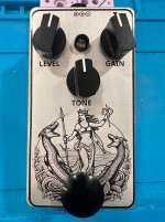
Here's my clone of the Barber LTD SR. I used the PedalPCB Sliver schematic, along with @Route14's Sliver -> Barber LTD SR component value swaps to turn it into a LTD SR ("Special Recipe"). I call it "Special Haircuts, LLC". I know, terrible name.
You might be thinking, didn't we just see such a build report? Yes, yes you did: Sliver Overdrive (Barber LTD SR). Right down to the same bare aluminum enclosure and graphics!
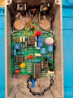
The main intent of this build was to be a test bed for my new mcu-bypass-firmware. I've come full-circle on bypass schemes. Years ago, I started down this road with a micro-controller (AVR Classic and PIC10F32x) based relay bypass. That was a true bypass scheme using mechanical relays (Panasonic TQ2-L2 and Kemet Kemet EC2-3TNU). That evolved into using a CD40106 or 74HC14 instead of the microcontroller to control the relay. The next scheme was Buffered Electrical Bypass that used a CD40106 for logic/control, and featured (buffered) electrical analog switching via the CD4053.
The latest scheme featured here unifies all approaches with microcontroller variants that support two different CD4053 (or TMUX4053) switching schemes: a simple scheme that I've always used, and a scheme with mute-while-switching capability. Additionally, there is a dual-latching mechanical relay variant. Right now the firmware supports the "AVR Classic" microcontrollers: ATtiny13a, ATtiny45, ATtiny85. I'm working on PIC10F320 and PIC10F322 support. Planned for the future is the next AVR generation, e.g. ATtiny202.
The big differentiating factor between this firmware and the former is:
Everything worked on first power-on... almost. It worked when engaged, but bypass only emitted a high-pitched/shrill noise. I could just barely hear the guitar, but it was entirely swamped by the noise. The mistake was laughably stupid: the through-hole CD4053 IC needs logic levels to be the same as the supply voltage (whereas the newer TMUX4053 can accept lower TTL or CMOS logic levels). The MCU runs at 5v, the rest of the circuit at 9 (or even 18) volts. To address this, the intent is to generally hold the switch control high via pullup resistor, and use a the microcontroller to drive a mosfet to ground on the same switch control line. Thus logic false is when the mosfet is "on" (via the microcontroller setting its gate high); and the logic true is when the mosfet is "off" and the switch pin is pulled up to voltage supply. The laughable part in this is that I went to all the trouble to design around the "MCU at 5v" versus "CD4053 at 9v" issue and then stupidly tied the pullup resistor to 5v instead of 9v! I'm pretty sure the high-pitched noise I heard in bypass was the sound of the switch oscillating rapidly, as the switch behavior at the "middle voltages" between positive and negative supply is undefined. What I've read suggests that CMOS logic circuits usually oscillate in this zone. So the fix was trivial, I cut the trace between the pullup resistor and the 5v supply, then ran a wire (on the back of the PCB) between that resistor and the 9v supply. Problem solved, and everything now works great!
Edit: a few other fun facts I forgot to mention initially:
You might be thinking, didn't we just see such a build report? Yes, yes you did: Sliver Overdrive (Barber LTD SR). Right down to the same bare aluminum enclosure and graphics!
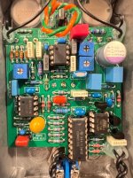
The main intent of this build was to be a test bed for my new mcu-bypass-firmware. I've come full-circle on bypass schemes. Years ago, I started down this road with a micro-controller (AVR Classic and PIC10F32x) based relay bypass. That was a true bypass scheme using mechanical relays (Panasonic TQ2-L2 and Kemet Kemet EC2-3TNU). That evolved into using a CD40106 or 74HC14 instead of the microcontroller to control the relay. The next scheme was Buffered Electrical Bypass that used a CD40106 for logic/control, and featured (buffered) electrical analog switching via the CD4053.
The latest scheme featured here unifies all approaches with microcontroller variants that support two different CD4053 (or TMUX4053) switching schemes: a simple scheme that I've always used, and a scheme with mute-while-switching capability. Additionally, there is a dual-latching mechanical relay variant. Right now the firmware supports the "AVR Classic" microcontrollers: ATtiny13a, ATtiny45, ATtiny85. I'm working on PIC10F320 and PIC10F322 support. Planned for the future is the next AVR generation, e.g. ATtiny202.
The big differentiating factor between this firmware and the former is:
- I'm taking advantage of the MCU's brownout detection and watchdog timers to handle rare/unusual situations (i.e. graceful reset rather than lock-up or other undefined behavior)
- I used AI to help me create an exhaustive testing and validation suite for the firmware; the core debounce algorithm is a "pure" implementation that is provably correct by formal methods, and can also be compiled on a general purpose CPU and tested extensively; the firmware itself is thoroughly tested via simavr, which tests just about every conceivable operational situation (WDT timeouts, corrupted stack, oscillator drift, BOD, EMI/too-bouncy switch, stuck switch, etc)
Everything worked on first power-on... almost. It worked when engaged, but bypass only emitted a high-pitched/shrill noise. I could just barely hear the guitar, but it was entirely swamped by the noise. The mistake was laughably stupid: the through-hole CD4053 IC needs logic levels to be the same as the supply voltage (whereas the newer TMUX4053 can accept lower TTL or CMOS logic levels). The MCU runs at 5v, the rest of the circuit at 9 (or even 18) volts. To address this, the intent is to generally hold the switch control high via pullup resistor, and use a the microcontroller to drive a mosfet to ground on the same switch control line. Thus logic false is when the mosfet is "on" (via the microcontroller setting its gate high); and the logic true is when the mosfet is "off" and the switch pin is pulled up to voltage supply. The laughable part in this is that I went to all the trouble to design around the "MCU at 5v" versus "CD4053 at 9v" issue and then stupidly tied the pullup resistor to 5v instead of 9v! I'm pretty sure the high-pitched noise I heard in bypass was the sound of the switch oscillating rapidly, as the switch behavior at the "middle voltages" between positive and negative supply is undefined. What I've read suggests that CMOS logic circuits usually oscillate in this zone. So the fix was trivial, I cut the trace between the pullup resistor and the 5v supply, then ran a wire (on the back of the PCB) between that resistor and the 9v supply. Problem solved, and everything now works great!
Edit: a few other fun facts I forgot to mention initially:
- I used BA282 clipping diodes. I really like these for clippers; I already had some, and just bought a bunch more from ebay. I'm not sure if they're real or not - they look a little different than the ones from the earlier batch. Now I can't remember why, but I have (or used to have) reason to believe the original batch is legit. But the new batch has a similar Vf as the original batch (per my DMM). The main thing I wanted was a Vf that's a bit higher than 1n914/1n4148, so I at least got that. Whatever they are, they sound good!
- This also (sorta) servers as a prototype for my quasi-IC module. In the past, my buffered bypass schemes used one half of the TL072 for an input buffer, and the other half for VREF buffering. This time around - and what I intend to do with the quasi-IC module - I gave up VREF buffering, and used the other TL072 half as an output buffer.
- As always, I like to push my builds into deliciously overkill territory. As I like to say, anything worth building is worth overbuilding. Here I used the PMOS reverse polarity protection scheme, no wet electrolytics (tantalum or organic polymer), 1 million cycle rated footswitch,
ferrite on power input, and hot-melt glue blobs on offboard wires for strain relief.
Attachments
Last edited: