- Build Rating
- 4.00 star(s)
One of the main reasons I build my own pedals is that I mostly enjoy the process. And I definitely find it satisfying to play through something I built myself. As such, the "more DIY" something is, the greater the satisfaction. And with pedals, that has been a progression of: kits, to PCB-only, to creating my own PCBs. (I think I'll stop short of casting my own enclosures or trying to make my own electrical components!)
Since I enjoy the act of building pedals, I don't see the time spent on it as a cost. So that means the price to try and audition lots of pedals is much lower than if I was actually buying commercial products. I suppose patience and working the used market might get me close to what I can do with DIY, but there are some pedals where even the used game is above my pay grade (for example, any Cornish pedal).
So I believe I've found my personal favorite circuit for a lead boost, the Catalinbread Varioboost. I came to this via my earlier PedalPCB Mercurial Boost build. Before that I was using a DIY GE-7 clone, the Effects Layouts Prismatic EQ. There's nothing wrong with the Prismatic/GE-7 for lead boost role, but I think they are a bit overkill for this specific purpose. I just want a slight overall boost, but a more pronounced mid frequency boost. I don't need to kill my bandmates with volume (that's the drummer's job), but I do want to stand out a bit. So I find the Varioboost/Mercurial to be perfect for this role.
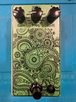
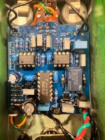
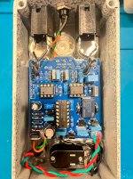
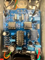
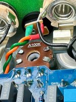
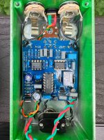
The Mercurial works perfectly fine and has served me well. But I always wanted all three knobs to be on the same horizontal line, and I wanted the bypass scheme to be integrated (for less/neater off-board wiring). I finally got around to designing my own PCB for this circuit, and here is the result. I liked the paisley-on-green aesthetic of my Mercurial build, so maintained it for this build. Loosely speaking, the upper half of the PCB is the Varioboost circuit, and the lower half is the inverter-based relay bypass scheme.
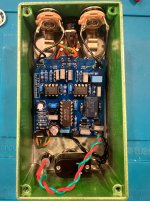
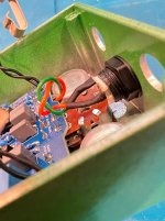
Everything worked on first power-on, but there are a couple minor issues that keep it from being perfect. One is that the PCB itself tends to "slant" down towards the enclosure. This is partially due to how I soldered the pots, but there is some implicit torque where the pots are soldered to the board, since they are all along the short edge of the board. Ideally I'd have a standoff or two between the PCB and the enclosure at the other end of the board. I think I'll probably just get some thick foam tape (like weather stripping) to put between the PCB and the enclosure.
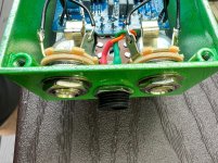
The other thing I failed to think through: the middle pot is a dual pot, so it's thicker than a regular single pot. That thickness, plus how close I drilled the pot holes towards the top of the enclosure, plus the fact that I used a full-size DC jack means that the DC jack is hitting that center pot, and actually sticks out of the enclosure by about 1mm or so. I could have avoided this by using a mini DC jack, or moving the DC jack hole up (to be on the same line as the IO jacks), or moving the pots all down a few mm. I'll probably leave it as-is, but the ideal solution would be to have some kind of bushing (preferably offset) so that I could use a mini DC jack. An "outie" DC jack would probably fix this too.
Edit: a couple other possible points of interest. The finish is a Sunnyscopa film-free waterslide decal. The transfer was ok, but not perfect, as you can see. I'm still wrangling with getting the process perfected with the new G1-PRO glue, as described here: Sunnyscopa Film-Free Laser Jet Waterslide Notes for New GW1-PRO Glue.
Circuit-wise, there's really nothing terribly exciting going on. But this is my second PCB with the RG Keen's Advanced Power Switching and Polarity Protection for Effects scheme. I first used this on my Egregiously Expensive Crunch (Cornish CC-1). This uses a low-RDSon p-channel mosfet for reverse polarity protection, instead of the typical series 1n5817. You can see the deliciously overkill Infineon IRFU5305PBF mosfet in the lower-left of the PCB.
Edit2: I have a few spare PCBs I'm happy to drop in the mail to anyone who wants one.
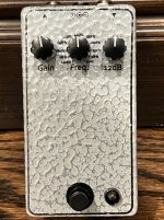
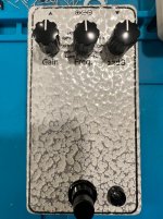
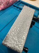
Edit3, Oct 1, 2025: Looks like I built the green one discussed in the original post in mid-July, 2025. So only two and a half months ago. It seems much longer than that! Anyway, I just built a second. The main reason I built a second is because I have two boards, and I wanted to replace the original Mercurial Boost I built with this custom version. I also wanted to try a build with one of these (new?) Tayda finishes, Silver Grey Hammer. The overall PCB build and electronic portion went together in a delightfully unremarkable fashion. But I'm kind of meh on the aesthetics. First off, I used the new Sunnyscopa GW1-Pro Glue... I used way too much (going against my own recommendation to use as little as possible). After transferring the decal, I tried to clean off the excess glue with acetone, only to find it started to remove the actual hammertone finish (it's hard to capture in a photo, you can kinda see it in the picture of the side below). So I was left with the decision to either leave the glue on, or remove it at the cost of scumming up the factory finish. The problem with leaving the glue on is that during the heat curing stage, the glue burns which (1) stinks up the house, and (2) turns brown and looks, well, burnt. The burning isn't terrible on this pedal, but I did another pedal with this finish at the same time (build not done yet), and it looks really bad with all the excess burnt glue. So I definitely like the original green paisley version I did much better. But this build works and does its job. Some day I'll probably make a third and go back to the paisley scheme. I did move the knobs down about 5mm, and also used a low-profile DC jack mounted alone the same line as the input/output jacks, so I had no pot-jack clearance issues this time around.
Since I enjoy the act of building pedals, I don't see the time spent on it as a cost. So that means the price to try and audition lots of pedals is much lower than if I was actually buying commercial products. I suppose patience and working the used market might get me close to what I can do with DIY, but there are some pedals where even the used game is above my pay grade (for example, any Cornish pedal).
So I believe I've found my personal favorite circuit for a lead boost, the Catalinbread Varioboost. I came to this via my earlier PedalPCB Mercurial Boost build. Before that I was using a DIY GE-7 clone, the Effects Layouts Prismatic EQ. There's nothing wrong with the Prismatic/GE-7 for lead boost role, but I think they are a bit overkill for this specific purpose. I just want a slight overall boost, but a more pronounced mid frequency boost. I don't need to kill my bandmates with volume (that's the drummer's job), but I do want to stand out a bit. So I find the Varioboost/Mercurial to be perfect for this role.
The Mercurial works perfectly fine and has served me well. But I always wanted all three knobs to be on the same horizontal line, and I wanted the bypass scheme to be integrated (for less/neater off-board wiring). I finally got around to designing my own PCB for this circuit, and here is the result. I liked the paisley-on-green aesthetic of my Mercurial build, so maintained it for this build. Loosely speaking, the upper half of the PCB is the Varioboost circuit, and the lower half is the inverter-based relay bypass scheme.
Everything worked on first power-on, but there are a couple minor issues that keep it from being perfect. One is that the PCB itself tends to "slant" down towards the enclosure. This is partially due to how I soldered the pots, but there is some implicit torque where the pots are soldered to the board, since they are all along the short edge of the board. Ideally I'd have a standoff or two between the PCB and the enclosure at the other end of the board. I think I'll probably just get some thick foam tape (like weather stripping) to put between the PCB and the enclosure.
The other thing I failed to think through: the middle pot is a dual pot, so it's thicker than a regular single pot. That thickness, plus how close I drilled the pot holes towards the top of the enclosure, plus the fact that I used a full-size DC jack means that the DC jack is hitting that center pot, and actually sticks out of the enclosure by about 1mm or so. I could have avoided this by using a mini DC jack, or moving the DC jack hole up (to be on the same line as the IO jacks), or moving the pots all down a few mm. I'll probably leave it as-is, but the ideal solution would be to have some kind of bushing (preferably offset) so that I could use a mini DC jack. An "outie" DC jack would probably fix this too.
Edit: a couple other possible points of interest. The finish is a Sunnyscopa film-free waterslide decal. The transfer was ok, but not perfect, as you can see. I'm still wrangling with getting the process perfected with the new G1-PRO glue, as described here: Sunnyscopa Film-Free Laser Jet Waterslide Notes for New GW1-PRO Glue.
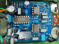
Circuit-wise, there's really nothing terribly exciting going on. But this is my second PCB with the RG Keen's Advanced Power Switching and Polarity Protection for Effects scheme. I first used this on my Egregiously Expensive Crunch (Cornish CC-1). This uses a low-RDSon p-channel mosfet for reverse polarity protection, instead of the typical series 1n5817. You can see the deliciously overkill Infineon IRFU5305PBF mosfet in the lower-left of the PCB.
Edit2: I have a few spare PCBs I'm happy to drop in the mail to anyone who wants one.
Edit3, Oct 1, 2025: Looks like I built the green one discussed in the original post in mid-July, 2025. So only two and a half months ago. It seems much longer than that! Anyway, I just built a second. The main reason I built a second is because I have two boards, and I wanted to replace the original Mercurial Boost I built with this custom version. I also wanted to try a build with one of these (new?) Tayda finishes, Silver Grey Hammer. The overall PCB build and electronic portion went together in a delightfully unremarkable fashion. But I'm kind of meh on the aesthetics. First off, I used the new Sunnyscopa GW1-Pro Glue... I used way too much (going against my own recommendation to use as little as possible). After transferring the decal, I tried to clean off the excess glue with acetone, only to find it started to remove the actual hammertone finish (it's hard to capture in a photo, you can kinda see it in the picture of the side below). So I was left with the decision to either leave the glue on, or remove it at the cost of scumming up the factory finish. The problem with leaving the glue on is that during the heat curing stage, the glue burns which (1) stinks up the house, and (2) turns brown and looks, well, burnt. The burning isn't terrible on this pedal, but I did another pedal with this finish at the same time (build not done yet), and it looks really bad with all the excess burnt glue. So I definitely like the original green paisley version I did much better. But this build works and does its job. Some day I'll probably make a third and go back to the paisley scheme. I did move the knobs down about 5mm, and also used a low-profile DC jack mounted alone the same line as the input/output jacks, so I had no pot-jack clearance issues this time around.
Attachments
Last edited:
")