jpants
New member
I really wanted my first post here to be a build report but alas, I require advice. I have some experience soldering on larger surfaces like guitar wiring but this is my first pcb attempt so I'm sure I'm making a lot of beginner mistakes.
I tried to read up and test as much as possible before posting but I'm running out of ideas of what else to test and I'm not sure that I'm making the right conclusions from the tests. So a huge thanks in advance to anyone taking time to read this and any pointers would be greatly appreciated.
I attempted to closely follow the steps outlined here although I didn't really test the circuit other than power to the LED before connecting the switch and jacks:
https://forum.pedalpcb.com/threads/basic-workflow-tips-for-building-a-pedalpcb.1165/


WHAT WORKS:
power, LED and switching work.
bypass signal comes through fine,
WHAT DOESN'T:
bypass signal is louder than effect signal but both are audible.
WHAT I'VE TRIED:
Everything that I tested here I've tested multiple times with a couple days off and some solder reflows in between. The first test was very similar to what I report below which are the results of the most recent tests. Originally, when I found signal with the audio probe everywhere I thought it should be, I assumed that my solder joints weren't good enough and reflowed what I thought were the worst ones. These pictures are all after the reflow, still not very good but definitely better than the first run.
I tested for continuity, I believe it blipped everywhere that its supposed to but I'm not 100% sure I was checking the right parts of the circuit. I double checked the values of all resistors, pots and caps as well as the orientation of all polarized components.
Audio Probe results:
I have signal (almost) everywhere that I think it should be:
- both sides of input cap C1
- top of R1, top of R3
- both sides of R2 and C2
- all 3 pins of the BS170
- both non-ground pins of A100k Volume pot
- but only the leftmost pin of C5k gain pot, should I also have signal on the middle pin?
Is there anywhere else in the circuit that I should be hearing a signal?
Voltage Test: I'm not sure what the correct values should be, but intuitively it seems wrong that I'm losing so much over D1, R1 and R5 since those just go to ground.
Whole circuit: 9.4v measured from power(+) to power(-) pads on pcb
D2: 0.12v
D1: 4.15v
R1: 4.15v
R3: 3.7v
R2: 1.3v
R5: 6.9v
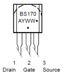
I also don't know what this should be and if I'm interpreting the pinout correctly but here's the voltage across Q1
BS170 (top down with LED up perspective)
Left-Middle (source-gate?): 0.26v
Left-Right (source-drain?): 1.57v
Middle-Right (gate-drain?): 1.3v
What should these readings be and what should I do to fix them? Is the large voltage drop over R5, D1 and R1 indicative of something grounding out that shouldn't be? I have other bs170s and backups of all components if swapping something might help.
I strongly suspect the culprit is my soldering, but I cant figure out which specific parts are the problem or if I've done damage to the board or other components at this point.
Additional newb questions:
Whats up with flux? I couldn't find a flux pen as described in the guide so I used a Jel Flux. Is that OK or should I be using something different?
--Thanks again for taking the time to read this.
I tried to read up and test as much as possible before posting but I'm running out of ideas of what else to test and I'm not sure that I'm making the right conclusions from the tests. So a huge thanks in advance to anyone taking time to read this and any pointers would be greatly appreciated.
I attempted to closely follow the steps outlined here although I didn't really test the circuit other than power to the LED before connecting the switch and jacks:
https://forum.pedalpcb.com/threads/basic-workflow-tips-for-building-a-pedalpcb.1165/


WHAT WORKS:
power, LED and switching work.
bypass signal comes through fine,
WHAT DOESN'T:
bypass signal is louder than effect signal but both are audible.
WHAT I'VE TRIED:
Everything that I tested here I've tested multiple times with a couple days off and some solder reflows in between. The first test was very similar to what I report below which are the results of the most recent tests. Originally, when I found signal with the audio probe everywhere I thought it should be, I assumed that my solder joints weren't good enough and reflowed what I thought were the worst ones. These pictures are all after the reflow, still not very good but definitely better than the first run.
I tested for continuity, I believe it blipped everywhere that its supposed to but I'm not 100% sure I was checking the right parts of the circuit. I double checked the values of all resistors, pots and caps as well as the orientation of all polarized components.
Audio Probe results:
I have signal (almost) everywhere that I think it should be:
- both sides of input cap C1
- top of R1, top of R3
- both sides of R2 and C2
- all 3 pins of the BS170
- both non-ground pins of A100k Volume pot
- but only the leftmost pin of C5k gain pot, should I also have signal on the middle pin?
Is there anywhere else in the circuit that I should be hearing a signal?
Voltage Test: I'm not sure what the correct values should be, but intuitively it seems wrong that I'm losing so much over D1, R1 and R5 since those just go to ground.
Whole circuit: 9.4v measured from power(+) to power(-) pads on pcb
D2: 0.12v
D1: 4.15v
R1: 4.15v
R3: 3.7v
R2: 1.3v
R5: 6.9v
I also don't know what this should be and if I'm interpreting the pinout correctly but here's the voltage across Q1
BS170 (top down with LED up perspective)
Left-Middle (source-gate?): 0.26v
Left-Right (source-drain?): 1.57v
Middle-Right (gate-drain?): 1.3v
What should these readings be and what should I do to fix them? Is the large voltage drop over R5, D1 and R1 indicative of something grounding out that shouldn't be? I have other bs170s and backups of all components if swapping something might help.
I strongly suspect the culprit is my soldering, but I cant figure out which specific parts are the problem or if I've done damage to the board or other components at this point.
Additional newb questions:
Whats up with flux? I couldn't find a flux pen as described in the guide so I used a Jel Flux. Is that OK or should I be using something different?
--Thanks again for taking the time to read this.


