First vero build - circuit works but output is barely audible.

zakco

Member
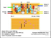
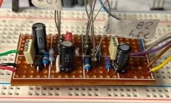
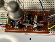
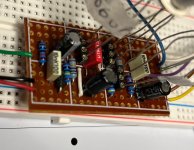
My first Vero build. It’s the Mind Bender as per this layout:
The only modification is the trimpot is wired off-board to a regular pot

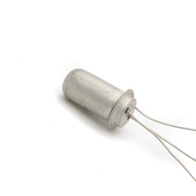
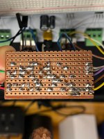
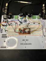
Voltages at all transistors are good, all controls function as expected but the output is barely audible - probably 30db quieter than it should be, but I can clearly hear that other than the output level, the volume, attack and bias pots are working. The gigantic GT404s make it difficult to see the top layout, but I've taken photos from a few angles, so hopefully everything is visible.

Any help would be appreciated, thanks!
 

Attachments

  • imgMINDBENDER VERO.JPG
    imgMINDBENDER VERO.JPG
    261.1 KB · Views: 15
  • IMG_3255.jpg
    IMG_3255.jpg
    490.1 KB · Views: 18
  • IMG_3256.JPG
    IMG_3256.JPG
    500.6 KB · Views: 15
  • IMG_3252.jpg
    IMG_3252.jpg
    322.3 KB · Views: 11
  • IMG_3253.jpg
    IMG_3253.jpg
    334 KB · Views: 11
  • IMG_3254.jpg
    IMG_3254.jpg
    340.3 KB · Views: 12
Last edited:
you said voltages are all good, but post them here anyway.

be sure to check the pinout on those GT402s. - i'm pretty sure they might be BCE (as opposed to the usual CBE)

also, I just had a look - GT402 are apparently PNP.

This circuit is designed for NPN Ge transistors.
 
you said voltages are all good, but post them here anyway.

be sure to check the pinout on those GT402s. - i'm pretty sure they might be BCE (as opposed to the usual CBE)

also, I just had a look - GT402 are apparently PNP.

This circuit is designed for NPN Ge transistors.
Thanks for your reply. I mis-typed - they are GT404(NPN) not 402. Sorry about that. I'll edit my post.
I breadboarded first and it sounded fantastic. The volume drop happened when I transferred the circuit to Vero. I'll post the voltages later tonight.
 
Correct. The pinout is a PITA, takes some creative bending to conform to the layout. I'll be shrink tubing those legs for sure.
The voltages are:
Q1: 7.4
Q2: 0.14
Q3: 7.5 (with bias control at noon)
im assuming the values above are collector voltages?

note: it's usually handy to know what the idle voltage is at each pin. e.g. Q1c, Q1b, Q1e (where c = collector, b = base, e = emitter)
 
I suspect ”schematic error” by solder bridge or missing/intermediate gnd connection somewhere.

IMG_8334.jpeg

Watch out for potential solder bridges between copper strips. Marked some of ’em. To exclude it being a problem run either an exacto knife couple times along area in between strips or do it with soldering station with a thin soldering tip, just be quick with going along trace gaps with tip avoiding taking solder of the copper trace itself.

Edit. JUST NOTICED SOMETHING TO EXCLUDE FIRST. You’re using sockets. Well there’s the problem most probably... Take ’em off and solder transistors back in RAW. No point in sockets IF you’re breadboarding. Then clean areas between copper traces and fire it up to enjoy your new pedal. :D
 
Last edited:
im assuming the values above are collector voltages?

note: it's usually handy to know what the idle voltage is at each pin. e.g. Q1c, Q1b, Q1e (where c = collector, b = base, e = emitter)

yes, collector voltages. Here's a complete measurement:

Q1c: 7.29
Q1b: 0.06
Q1e: 0
Q2c: 0.14
Q2b: 0.07
Q2e: 0
Q3c: 7.5
Q3b: 0.15
Q3e: 0
 
I suspect ”schematic error” by solder bridge or missing/intermediate gnd connection somewhere.

View attachment 119935

Watch out for potential solder bridges between copper strips. Marked some of ’em. To exclude it being a problem run either an exacto knife couple times along area in between strips or do it with soldering station with a thin soldering tip, just be quick with going along trace gaps with tip avoiding taking solder of the copper trace itself.

Edit. JUST NOTICED SOMETHING TO EXCLUDE FIRST. You’re using sockets. Well there’s the problem most probably... Take ’em off and solder transistors back in RAW. No point in sockets IF you’re breadboarding. Then clean areas between copper traces and fire it up to enjoy your new pedal. :D

As this is my first non-pcb build, I didn't want to commit until I knew my vero work was solid. It took me a while (and expense) to find suitable NPNs for this circuit and if I biffed the vero layout in some tragic manner, I didn't want to risk destroying the transistors by desoldering! So, you believe that sockets are so inherently problematic, that they're more likely the issue than a solder bridge?
 
Back
Top