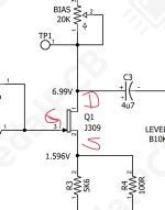
I am building the Fumble boost. I need to know how to read the jfet pins on the schematic.
Interfet n-channel j309 data sheet has
1 source
2 drain
3 gate
How does one determine the jfet pinout on the schematic?
Is it safe to assume schematic is
1drain
2 source
3 gate?
thank out
Interfet n-channel j309 data sheet has
1 source
2 drain
3 gate
How does one determine the jfet pinout on the schematic?
Is it safe to assume schematic is
1drain
2 source
3 gate?
thank out

