More Skeptical Buffer Wiring Issues

BQFS

New member
The fun never ends. I just finished drilling all the holes and mounting the hardware, so all that remains is to wire it up, and that's when I came to a dead halt.

For clarity, this appears to be a Rev 1 board, due to the components and layout, plus the switches are closer together compared with the newer drill template.

Here we go:

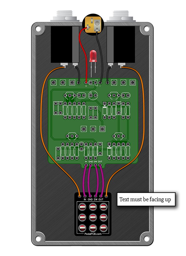
At the top of the board, nearest the power jack and in/out jacks (all top mounted as per the template), there are four holes, all with no label.
At the bottom of the board, nearest the stomp switch are four more holes.

On the SB wiring diagram, there are six holes at the top and four at the bottom, all labeled.
Since nothing was labeled, I hate to assume, so I put the meter on continuity and found the following:
Let's call the holes 1-4 starting from left to right.
At the top of the board, holes 1 and 2 are together, and are connected to hole 3 at the bottom. My guess is that one of the two holes at the top receives power from the jack and the other provides power to the onboard CLR, sheer guess.
At the top of the board, hole 3 does not appear to connect to anything, but hole 4 also connects to hole 3 at the bottom.

It would REALLY be helpful to obtain a schematic (page 4), wiring diagram (page 5), and component value pictorial (page 2) for the Rev 1 board I actually have. Newer versions just don't appear to be close enough to generalize.

I am not the world's greatest visualizer so as I often do, I picked too small an enclosure, so everything is a tight fit. I suppose, if I have to, I can remove the board from the enclosure and trace the wiring manually, but I am hoping I am not the only one who found themselves in this boat.

Also, I got conflicting advice about the output resistor R13. On the schematic I have, it shows a 10 ohm resistor. On the board, it shows 100K - quite a difference. One person on the forum told me to use the value on the board (100K) and another told me to disregard that and use 10 ohms, which I did. That much difference should certainly make a huge difference in the amplitude of the output, so does anyone know which value I should be using?

Finally, I had intended to use one of those large blue stomp switches, which I have way too many of, since it has the built-in LED, but it is too big to fit, so I have gone back to a regular-size switch. Normally, I would use the PPCD daughter board, but I only have one left (I already soldered my second-to-last one to the big blue switch) and don't want to use it if there is no 1-1 relationship between it's holes and the ones on the board.

If I use another outfit's daughter board, I can more easily wire up the input and output jacks, plus it makes it a LOT easier to wire up an LED near the switch. I have NO idea where to put an LED if I can't do it that way.

In my own defense, I didn't buy this board directly from PPCB. I ran into a guy on Reddit who said he had ADHD and was getting out of building pedals. I bought a ton of stuff from him, and this board was part of that.

Okay, I will shut up now and hope for some very much appreciated assistance. Thanks in advance. I suppose this is what I get for using an out of date board.

Bud
 
First off, you are not alone.

Many people jumped on this circuit as soon as a PCB was available.
The info you seek is on the forum, some of same said info you may have to hunt for it yourself.

I believe I have the early rev as well. I've marked on my copy of the build doc that

"Even if the PCB says it's 100k, it's 10r"

Also on my doc, lacking the schematic "Revised 2/29/24" (latest rev currently online is "Revised 4/24/24",
on the PCB image with REFDES — Next to R13 in GREEN, I've marked it as "10r".

This would be one of those exceptions to the rule that "whatever the doc says, go with what's on the board" —
in this case, go with the 10r


For wiring up the effect-loop, here you go.

For wiring up the top four holes of the board, when you said: "Let's call the holes 1-4 starting from left to right." — is that left to right looking at the component-filled side of the board? Probably, but it doesn't hurt to make sure by asking because you said that 1 & 2 holes are together and connected to 3 at the bottom — leads me to believe you're looking at the "nibs"/solder-side of the board or you've got a SOLDER-BRIDGE BETWEEN 1&2 because...

Looking at the populated side of the board, top four holes:
G + - G
◉◉◉◉

1&2 should NOT be connected.
The outer holes are for running a ground wire to your I/O jacks' grounds.
So the "-" should show continuity with the outer holes, the last two holes at the top (and the first), if looking at the populated side, should be ground.

Check the second hole, "+", with your continuity tester and make sure it's going to D100, a 1N5817. If it is connected to the other holes then you have a solder bridge and must reflow solder and in that process destroy the bridge.


At the bottom of the board, looking at the populated side:
IN G SW OUT
◉ ◉ ◉ ◉


Those 4 holes on the motherboard correspond to the middle four holes of the 3PDT breakout board (IF you've got the standard breakout-board and not mistakenly trying to connect either of the BUFFERED 3PDT breakout or the KLON-3PDT breakout boards.

The Standard 3PDT Breakout holes are thusly:

IJ IN G SW OUT OJ
◉ ◉ ◉ ◉ ◉ ◉

So, that 3rd hole should have continuity with holes 1,3&4 at the top — they're all ground.

"IJ" — run a wire from the "tip" of your in jack
"OJ" — run a wire to the "tip" of your out jack
THE MIDDLE 4 of the 6 SHOULD LINE UP STRAIGHT ACROSS to the bottom 4 of the main-board.


The PPCB standard 3PDT breakout boards ground the circuit's input on bypass, so you MUST solder the breakout board on its correct side to your 3PDT-switch. If flipped, it won't work properly.

With your continuity-tester, check the breakout board's hole for pin-1 of the 3PDT, it should connect to where pin 6 goes.

1 4 7
2 5 8
3 6 9


Here's how you'd wire it without the breakout board:
PEDALPCB 3PDT wiring for PCBs that connect directly to in:out jacks.png

3PDT.png


If you ever have to start another troubleshooting thread...

POST PICs!

That is standard operating procedure in the troubleshooting forum, because it is much easier to see what may be wrong than to interpret someone's description of it.
 
Okay, thanks for that thorough reply. Here's a picture.

At the top of the box, between the jacks are the four holes in question. The two outside holes are connected, and the two holes on the left are also connected. So, the outer two are Grounds. If the hole second from the left is (-) or negative, perhaps that just means that the negative hole is tied to ground. Begs the question, why call it negative in the first place. Or there is something wrong with the board. As you can see, there are no solder connections to any of those holes because I had no idea which hole was supposed to connect to what.

I had to take a second shot because the daughter board (obviously not soldered on yet) was covering the four holes at the bottom of the board.

Sometimes I work on things later at night than I should, and end up overlooking things. This one is no exception.

I removed the board from the enclosure and turned it over. Sure enough, in very small letters, the holes at top and bottom were labeled.

The top ones, viewed from the solder-side are Gnd Neg + Gnd just as Feral Feline indicated. The bottom ones, again viewed from the solder-side, are labeled, left to right, are OUT SW G IN.

So that means, if I use the breakout board, I will need to cross the G and SW wires. Whomever designed the board really missed that. The holes on the board should have been oriented the same way as the switch board. Likewise, it would have made more sense to label the holes on the side that is visible when the unit is being assembled. Oh well. Maybe they changed that in subsequent revisions.

Because it is such a tight fit, I think I will forego using the daughter board, and just wire up the switch as shown, and put the LED at the top of the board as well. That should take care of it.

Thanks again for your help. I will change the thread status once the board is together and working. Still have a ways to go, and of course, not having learned my lesson, I am still going to stay up late to complete it.


Skeptical Buffer.jpg
 

Attachments

  • Skeptical Buffer 2.jpg
    Skeptical Buffer 2.jpg
    286 KB · Views: 6
Begs the question, why call it negative in the first place. Or there is something wrong with the board.

The - pad is for the negative terminal of the DC jack.

The two GND pads are for the grounds of the In / Out jacks. They are all connected together and interchangeable.


Now the bad news, then the good news.

Your PCB is mounted upside down and the toggle switches are on the wrong side of the PCB. The components should be facing you when looking into the enclosure. Because of this you'll need to modify the wiring diagram above

The good news is that since this PCB has no potentiometers it will behave exactly as it should, nothing will be inverted once it's wired up correctly and you won't need to remove the toggle switches.


If no one beats me to it I can draw you a modified wiring diagram tomorrow, I'm on a phone at the moment.
 
This is hilarious. I generalized my knowledge from the other builds, as they had the controls mounted on the soldering side, so without thinking about it, I just did the same. Well, there were clues, and now I know what to look for if (hopefully, but more probably when) this happens again. Now, of course with hindsight, it makes sense that the print identifying which hole is which was on the opposite side. (Sound of hand smacking forehead).

No worries. And thank you very much for pointing this out. You are so right, should have posted the pics first, but thanks for the "bad news." This will definitely help in the future.

I am an ace at desoldering, years of experience, so I think I will go ahead and move the switches to the other side of the board. Pennance for screwing up and not even realizing it. Oh boy....

Bud
 
I don't know if you're following this any longer, or if indeed anyone is going to read this, but the build had one final problem. I had no problem desoldering the switches and moving them to the other side of the board. Then there was figuring out how long to make the leads for the LED, but before I soldered them in place, I wanted to make sure the pedal was still working.

I plugged in my bench 9V supply and pushed the stomp switch. No LED. Pushed again, no LED. Hmm. I consulted the schematic and made sure I was getting voltage to the anode, check. So, that left the SW connection. It was wired to the correct hole on the daughter board. So, I measured for continuity and it turned out that the DAUGHTER BOARD was to blame! There was no physical connection between the SW hole and the top middle switch lug. So, I desoldered the wire from the SW hole and soldered it directly to the top middle lug. Voila! What a weird failure!

I don't think I will be ordering any more of those boards. Just as well this was my second to last one. Before I use the last one, I'm going to measure to make sure all the circuits function as they should.

Well, I sure learned a lot, and I guess that's what counts. I can see why some people think the switches are all fake. I play bass, so I am not sure any of the positions make any difference. We'll see. Tomorrow, I give it a road test on my gigging pedal board. Going to put it first, right after the compressor and hear what happens.
 
...Sometimes I work on things later at night than I should, and end up overlooking things. This one is no exception.
...

We are siblings separated at birth.

You've been through the school of hard knocks, but your lessons are burned in for good now, I bet.

I'm glad I said "Looking at the populated side of the board..." 😸

PedalPCB's designer has vetted all his designs extensively, and numerous builds have been made by numerous people without problem.
SO, I suspect either you got a dud-daughterboard (they happen), or something else is going on that most likely involves human error.

You can see why pics are so important, now.
I'd like to see updated pics of both sides of the board.
If you inadvertently damaged a trace on any of the switches, that could account for them sounding like they aren't doing anything — because maybe they're not!

More likely, the changes the switches make are subtle, made even more subtle when used with a bass. If you've got a lot of effects, then it's probably still worth having on your board even if the switches don't do much. For mine, I plan to make full use of the loop for Fuzzes that don't play nicely after a buffer (that's kind of the main point of the loop, I think).


I look forward to hearing your thoughts on it after your road test.
 
I am VERY glad you made that comment about the switches being on the wrong side. As you say, I learned quite a few lessons building this otherwise simple pedal. I didn't see that you could build in an effects loop until it was too late. If I re-house the pedal, which I may do, then I will get a larger enclosure and build in the loop. That's a great idea, and thanks again for pointing that out.

As I posted in my other thread on the same subject, the switch daughter board is definitely defective. The trace is supposed to be hard-wired from the SW hole to the top middle lug of the switch. It isn't. My meter tells me it is a completely open circuit. When I moved the wire from the SW hole and soldered it to the top middle lug, the LED started acting correctly.

What's ironic about that is that at first I thought I would do without the board as wiring it manually didn't seem like that big a deal. Until I started to do it and then it became one large pita. So I ended up using the board anyway, although I had already decided to attach the LED to the buffer board, rather than the daughter board because there wasn't enough room to squeeze the LED between the bottom of the switch and the edge of the enclosure. Even so, using the daughter board was much easier than wiring up the switch manually. Duh.

I didn't see your last message until I had the unit back in its enclosure, screwed together, and installed on my pedal board. So, unfortunately, no chance to provide pictures of the board itself. The board, however, clearly works just fine, although, for a bass player, the switches are of minimal value. If I had to build this one again (and I may because I hate the ugly way I had to use large washers to cover up the too large switch holes), I will use jumpers to put the switch circuits into always on and not need to drill holes for them, saving the very minor cost of three switches, and making for a very clean-looking enclosure with just an LED and stomp switch on its top side.

Road test completed. With each switch, there is some difference in tone, just not very pronounced. I just put all three switches into the On position and plan to leave them that way. I stand by my previous statement. The unit works great as a buffer, but the switches, as far as I am concerned, could have been left off.

I plan to use the buffer as an always-on pedal, immediately following the compressor. I have a bunch of effects pedals, but use each sparingly and rarely in combination. I was motivated to build a buffer due to too many true bypass pedals in the chain. In fact, going one step further, I could easily wire the pedal with no switches at all, and make it, literally, an always-on pedal.

My favorite pedal, at the moment, is the new Fender Bassman Reverb pedal, designed for bass. It has a very accurate and highly useful HPF which keeps the pedal from making (as one player put it, referring to most reverb pedals attempted to use for bass) me the "Mayor of Mud City."

Thanks again for your assistance and great suggestions.

Bud
 
Iron Ether has a great Bass Reverb pedal (never owned it, alas); but that Fender Bassman Reverb seems similar — I'll have to see if I can try one somewhere.

I'll be using my Skeptical Buffer in much the way you're using it, save for the loop as mentioned earlier.

BTW, it was Robert who pointed out your PCB was backwards; I came back to the thread after that but would've told you the same thing.

You've mentioned several times in both your threads that the breakout-board is defective because there's no connection between "SW" and Lug-4;
there is NOT supposed to be a connection there. :dmm:

Whether the regular 3PDT Breakout Board or the Illuminated 3PDT Breakout Board Single Colour (which is what you have in your build here),
to reiterate:
there is NOT supposed to be a trace hard-wired from the "SW"-hole to the top middle lug of the switch. 🤷‍♂️


The breakout-board in your build is meant to be used with a 3PDT switch that has its own LED-Ring (but your breakout board doesn't have to be used with one, a regular 3PDT is fine):


Good vid that explains in general how a 3PDT footswitch works, in addition to how the LED-RING is configured (Skip to 4:00 to see it light up).

Here's the Illuminated Breakout Board you have and all its traces outlined:

3PDT-Illuminated-1 (single colour) breakout board PedalPCB.png
 
Last edited:
"
"You've mentioned several times in both your threads that the breakout-board is defective because there's no connection between "SW" and Lug-4;
there is NOT supposed to be a connection there" -

That's NOT what I said. I said that the trace on the daughterboard was open. Normally, there is a direct connection between the SW hole on the daughterboard and the lug that is top center.

Obviously (well, maybe not so obviously) the trace doesn't go to the lug, that would be impossible. I didn't know how to describe it without using a million words, but what I meant is that there is a trace that connects the SW hole to the circuit loop that is soldered to the top middle lug once the daughter board is installed and soldered to the switch.

I omitted all those words because I assumed (oops) that most people familiar with the daughter board would know what I meant, and would understand I didn't actually think a circuit board was hard-wired to a switch lug.

I apologize for creating that misunderstand, but now you know why I phrased it the way I did.
 
Back
Top