Muffler no gate

Markk

New member
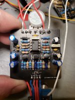
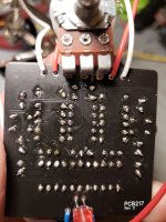
Muffler noise gate has no effect. I have signal through the circuit, but it's regular clean.

Here is my voltage

IC
pin 1 4.5
Pin 2 4.5
Pin 3 4.4
Pin 4 0v
Pin 5 4.3
Pin 6 4.5
Pin 7 4.5
Pin 8 9.1

Q1
Pin 1 3.6
Pin 2 4.1
Pin 3 9.1

Q2
Pin 1 0v
Pin 2 0.1v
Pin 3 0.2v

Q3
Pin 1 4.4
Pin 2 4.5
Pin 3 0.2
 

Attachments

  • 20221004_192029-min.jpg
    20221004_192029-min.jpg
    862.2 KB · Views: 16
  • 20221004_192059-min.jpg
    20221004_192059-min.jpg
    809.5 KB · Views: 16
Hey I see you got no help on this...

I'm no expert, but looking at your voltage, I think you VREF_B voltage is wrong. From what I can understand on the schematic, VREF_A is a voltage divider so it should be at 4.5V which you have, but VREF_B with a 5V1 Zener diode should be at 5.1V...

I would check that part of you voltage circuit. If you get 4.5V on Q3 pin 2, then you VREF_B seems to be at 4.5V, which would be the same as VREF_A and I wouldn't see the point of having two different ref voltage circuit if they were the same. So that makes me think your Zener it's not doing its job.

Also near zero on all pins of Q2, seems abnormal. I checked your values from VREF_B to Q2 pin 3 and R10,11 and 12 are right. I can't confirm C6 and C5, so I would double check that if I were you. You might want to check your voltage on each side of R11... I think you should read near 5V on each side...

Just a few pointer that may help....
Thank you sooo much, will check those items and report back!
 
Hey I see you got no help on this...

I'm no expert, but looking at your voltage, I think you VREF_B voltage is wrong. From what I can understand on the schematic, VREF_A is a voltage divider so it should be at 4.5V which you have, but VREF_B with a 5V1 Zener diode should be at 5.1V...

I would check that part of you voltage circuit. If you get 4.5V on Q3 pin 2, then you VREF_B seems to be at 4.5V, which would be the same as VREF_A and I wouldn't see the point of having two different ref voltage circuit if they were the same. So that makes me think your Zener it's not doing its job.

Also near zero on all pins of Q2, seems abnormal. I checked your values from VREF_B to Q2 pin 3 and R10,11 and 12 are right. I can't confirm C6 and C5, so I would double check that if I were you. You might want to check your voltage on each side of R11... I think you should read near 5V on each side...

Just a few pointer that may help....
I have 4.5 one one side of r11, then 0.1 on the other..
 
Back
Top