You are using an out of date browser. It may not display this or other websites correctly.
You should upgrade or use an alternative browser.
You should upgrade or use an alternative browser.
Need Wiring Diagram for 3PDT Breakout Board with Output Boost
- Thread starter StudHaus
- Start date
Feral Feline
Well-known member
You might be overthinking it.
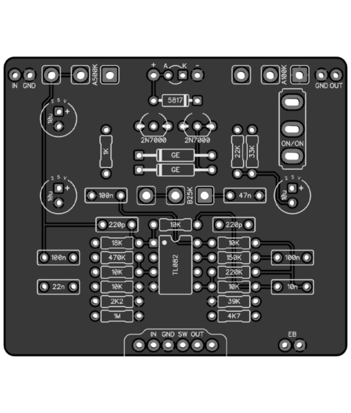
If you're hooking it up to a PedalPCB board (most any of them, but not all), it's very straightforward...

POWER should be straightforward enough, so I left that off the diagram.
As you can see, there are a couple of places to wire up the IN/OUT jacks.
If you're hooking this 3PDT Boost-Board to Perf, another vendor's PCB, or (*shudder*) vero, it can still be hooked up but may not be as clear how to do so.
Whatcha makin'?
StudHaus
New member
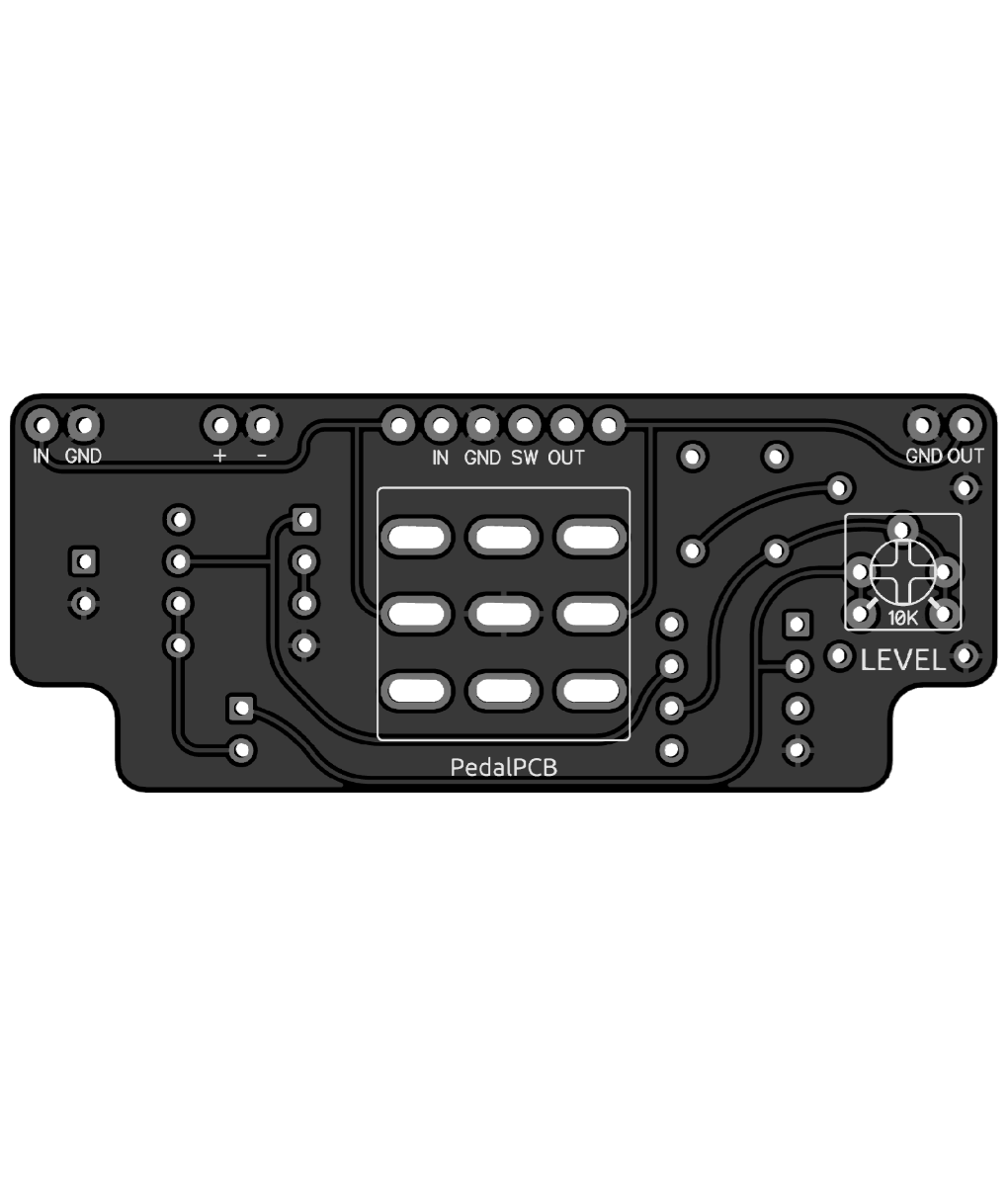
Blue breaker with breakout boost: all PedalPCB boards, no 9v battery clip. Should be extremely simple.
I do not understand the green cables going to the FW, it seems redundant and potentially very messy.
Would you mind explaining what's going on there and if it's really necessary?
Why is there no wiring diagram or BOM for this board?
I do not understand the green cables going to the FW, it seems redundant and potentially very messy.
Would you mind explaining what's going on there and if it's really necessary?
Why is there no wiring diagram or BOM for this board?
mkstewartesq
Well-known member
I take it the diagram means that you can plug the wires from the input and output jack to either of the in/out pads and the signal will get to the appropriate place it needs to be on the foot switch. You don’t need to wire up both and you don’t need to do any any additional wiring between that pad and the foot switch. As noted, you have multiple pads and ground options because you may be using this with some board (or Vero) that isn’t as straightforward to wire as a PPCB boardBlue breaker with breakout boost: all PedalPCB boards, no 9v battery clip. Should be extremely simple.
I do not understand the green cables going to the FW, it seems redundant and potentially very messy.
Would you mind explaining what's going on there and if it's really necessary?
Why is there no wiring diagram or BOM for this board?
As far as why there is no BOM, I suspect it’s because none is needed. The only component to be added is a 10 K trimmer and that’s shown on the board.
Edit to add – actually, sorry, I do sort of see your point about the bill of materials because I have no idea what all those other pads are for and it’s not clear from the board. So I didn’t mean to insult your intelligence with my comment because I just wasn’t looking as closely as I should’ve been.
Robert
Reverse Engineer
Both aren't necessary, you have two options, use whichever is more convenient for the PCB you are building. (In this case, the outer pair)
The wiring will look identical to the standard 3PDT breakout board wiring, with the exception of the 9V / GND power connection which should come from your DC jack.

The wiring will look identical to the standard 3PDT breakout board wiring, with the exception of the 9V / GND power connection which should come from your DC jack.


StudHaus
New member
THANK YOU!! I think I got it now, i was just confused with the "extra" pads next to the usual "IN, GND, SW, OUT."
So just to confirm:
1. "IN, GND, SW, OUT" bottom of Blue Breaker board -> "IN, GND, SW, OUT" on Breakout Boost board
2. "-" and "+" from Breakout Boost board go to the 9v power jack. (this powers both boards?)
3. "GND" and "GND" from Breakout Boost board go to the two 1/4" jacks (as usual).
Are there ANY other connections that need to be made?
Do the 9v pads from the Blue Breaker PCB also go to the power jack, or is it unnecessary because of the 9v connections made on the Breakout Boost board? Might be tough to fit those additional wires into the tiny holes of the 9v jack...
Thanks again, I really appreciate all your guys' help.
Robert
Reverse Engineer
THANK YOU!! I think I got it now, i was just confused with the "extra" pads next to the usual "IN, GND, SW, OUT."
The extra pads pair up with certain PCBs, like the ADHD.
So just to confirm:
Correct, except both PCBs need power.
If you can't fit both wires into the DC jack lugs you can install one like normal, then "surface mount" the other wire to the side of the lug.
Feral Feline
Well-known member
Hey StudHaus, I guess you've got it sussed now.
In my post I just showed the paths on the PCB in green to illustrate the routing, I should have made it more clear that either sets of pads could be used.
In my post I just showed the paths on the PCB in green to illustrate the routing, I should have made it more clear that either sets of pads could be used.
Robert
Reverse Engineer
Is there a way to wire it as a separate boost?
If you jumper the IN / OUT pads together (in the IN/GND/SW/OUT cluster) you can use it as a standalone boost pedal.
Just drop it in an enclosure and wire up the jacks.
I’m planning on putting one in a Clandestine Boost. I want a little more volume to use it as a crunchy boost and I’m hoping this little board will do the job. I’m just trying to decide if I want to add a pot that I can adjust externally. And where to locate it.