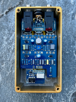
Chuck D. Bones
Circuit Wizard
That's good.
Nice! Where’d ya get that sweet enclosure?
In my basementNice! Where’d ya get that sweet enclosure?


I used these knobs from Tayda. Just make sure to use spline shaft potentiometers. The enclosure is Tayda's Metallic Dark Gold. I should probably get around to doing a build report for this one.@PedalBuilder Very nice! Looks like the same Tayda color used on my MB Cosmopolitan (Screwdriver). This is for sure at the top of my list. Where’d you find the knobs? I bought some silver ones but they’re a little small for my liking…plus there’s no indicator on top which is a must for this kind of pedal!
Thanks! They're my own designs and I don't have a website. The gerber file for the Hybrid Fuzz Driver Deluxe PCB is available here. If you're interested in any of my other PCBs, feel free to message me directly.@PedalBuilder - where do you get these Naegele Audio PCB's? I don't find a source w/ internet search engines...
TEACH US YOUR WAYSIn my basement. 100% DIY.
