Tube Preamp PCB (draft)

pbrommer

Well-known member
Good evening -

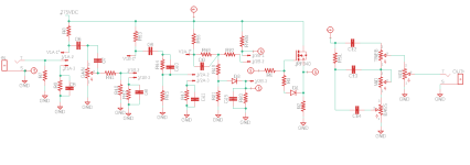
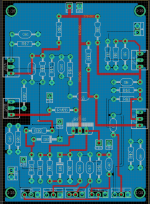
I like making perfboard layout of preamps, but I'm kind of nervous of the longevity of some of them (one is working, but the ground and +250VDC are literally millimeters apart!) . So, I've taken a shot at putting together a 125B sized (but no tubes!) layout for 2 tubes plus a (gasp) MOSFET CF option. There are many options and extra parts, just in case you want to build them out. If you would all kindly take a look and see. I can't see any major issues -- it's not the prettiest and balanced, but I think it will work. Let me know your thoughts. EagleCPB (I know, but I get it free at work!) and schematic are attached.
simple preamp schematic v.1.png simple preamp layout v.1.png
Couple notes:
1. There is a plate TS out and cathode follower TS out. This is due to some amps use plate driven tonestacks (Fender) and other use cathode followers (Marshall).
2. The +275VDC will come from a SMPS board.

Patrick
 
From the schematic, at a quick glance, it's a modular 2 tube pre that should work. I wouldn't expect tons of gain out of it.

Regarding the PCB tho, and while I am not sure which scale you are using, there are some issues with your blue side imo. Putting aside the fact that I am not a big fan of ground pour when you have high voltage and AC in the mix, you don't have enough creepage between traces and plane but especially pads. I suppose you are going THP, so that means your pads will be on both sides - you need your creepage rules there too! So all pads seeing 250VDC need space from your ground pour and from other tracers (say 3-4mm). And also for traces: for example if you look at RV2B (that you might jump even) you seem to have a trace that goes to a pad. You might have 250V on that one and there is virtually no creepage (or am I reading it wrong?) If you power this with what you plan for, you will fry the board. And if the 1-16 on the corners are holes (platted?) for standoff, you are going to fry something else.

imo you should (respecfully) have another go at it but write down on each trace what the min and max expected voltage will be, then try to layout component and traces with proper creepage. You have a lot of room on the top side, use it.
 
Cool. I went ground pour on the bottom side trying to keep the big VDC on the top. No way I wanted to pour copper with those big traces. And you’re right, there are some big voltages there on the blue (bottom side). I’ll look at that - don’t know what I was thinking.

The 1/16 (whatever that label is) is for mounting hardware.

Thanks for the feedback - just giving it a shot. I like what Merlin did with his 12ax7 PCBs, and wanted to have something similar. I can always make it a bit larger too - give myself some leeway.
 
As long as you respect creepage, you won't have an issue putting VDC and signal on the same plane. Usual rules apply: no parallel traces etc. Also short traces beat everything - you are almost exclusively using 90° turns while the norm is usually 45° turns. For example your R19 / D3 / R21 connection could be made much better that way. 90°+ turns also create "electron hot spots" which isn't good. If you keep 90° try to smoothen them with a small 45° inclusion.
 
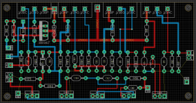
So, I gave it another shot, this time in landscape. Little wider and narrower. Guess I went Hiwatt style. :)

1763697022692.png
I did move some of the potentiometers from the bottom up a couple millimeters (my grid is in 1mm squares). Everything should have 1.5-2mm clearance, all HV is on 1.25mm traces, and I put the grids and cathodes on the underside for convenience. I just need to think about how to ground it all. Thanks for the feedback everyone. I'm giving it my best.
 
Looks better already. You have a few parallel traces on the same PCB side I am not a fan of (gain pot for example) and some surprising choices of component connections (why do C9 - C10 - R14 and not C9- R14-C10? Doesn't change a thing for the electrons, but you'll save some trace length).

More generally, 1.25mm trace width is massive overkill for 12ax7. They use low amps and you could half the width without any thermal issues. In a small form factor and at this voltage, voltage drop will be minimal anyway. Signal traces can easily be 0.5mm too. That will give you more creepage which is always good.

For your pots, what are you trying to achieve? It seems to be very small footprints. Are you going for PCB mounted pots, or are you going to wire them out? You could save some traces headaches by using of board components for the tone stack, including a ground bus. And increase spacing between pads.

As for your ground, in that case I would run 1 to 1.5mm wie trace as a bus through the PCB. Assuming what is not connected here is ground, you could move the bottom traces to the top, and run a ground bus on the bottom trace "below" your row of component with smaller 0.5mm connection to individual pads as needed. Care for ground loops obviously.
 
I shouldn’t probably post when I’m a bit tired: I forget context. And yes, you’re right: the airwires are Ground connections.

1. I calculated 1.25 somehow, but I’ll probably move it to .75-.85, just to give myself a bit of leeway.
2. Good thoughts on the signal being smaller width.
3. The parallel traces are the grid and cathode connections to parts. And connection wise, I probably was just placing and thinking. I’m sure there’s some efficiency I can achieve. I’ll look at the potentiometer area again.
4. The goal for the potentiometers was just a place holder. I will be off-board wiring them to the panel. I did this off of the other preamp PCBs I had from Merlin with no issues. I’ll fiddle with the layout.
5. Thanks for the grounding idea. I thought about that as I was falling asleep.
 
Self reply. Man, I always screw up where ground loops would/would not be. I’ll give it a shot and have you tear it apart. :)
 
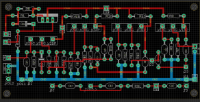
As my college football team was getting its teeth kicked in, I decided to work on this layout. Here's revision 3. I think, think there's at least 2mm between traces/holes. I used pads for the tone stack (I know, that part isn't pretty). I also moved the 275v to the top area of the board (with 3mm from edge), which I think made it a bit more compact and efficient. I tried to keep all plate/cf/interstage connections from plates at .81mm and everything else was 0.6mm. 1.27 grounding buss. Looks like I could change the connections from the cathodes to 0.6mm. Thanks a bunch for the feedback everyone.

1763868578672.png
 
Looks good. You still have a couple of parallel traces that might be close enough to couple (thinking D3-R19 area). Might want to swap some traces to the other side there, the PCB thickness will help with that.

Having the soldering points a bit far apart for the pots isn't a big deal but make sure they don't act like big antenas - get them as close as you can together and twist.

The cathode traces I personally like to keep around 0.75 and as short as possible (their voltage is important and I am just ensuring lowest voltage drop possible) but what you have is fine.

Be careful that your ground injections/and lifts to enable cathode followers for example doesn't lead to ground loops. I would put a few more ground pads on the main ground trace, so you have flexibility without having to think too hard.

What you could do is use some kind of pin connector for the tubes, making sure they are properly 300+ rated. Same for the supply, which currently doesn't seem to have pad distance high enough. Molex, TE etc have some iirc.

Also, don't forget that your mounting holes generally will have a washer / locking washer much larger than the actual hole. I see T3, R8 and R1 might be an issue.

Your board as it is will work, to me the remaining concerns are the power supply pad distance and potential ground loops. The optimization I would do is taking care of parallel traces on the same side and put them on the other side. And if I were to start from scratch, I would with your general idea put the tonestack off-board, grid stoppers off board and probably try to get the tube connections side of the board for convinience and lowest noise.
 
I did try the tube connections on the edge of the board, but it got kind of clunky.

I like the idea of of the grid resistors off board, especially since it will just be for myself. And the parallel trace in that D3/R19 was a “I know it’s parallel but I can’t make the layout any prettier” moment.

Oh, I did make another change (after this picture) to shift the tone stack connections to the middle of the board. I also removed the OUT connection to be off board as well.

I’m getting there. Then when it looks good, I’ll give them some prototyping. Thanks for the feedback.
 
I like the idea of of the grid resistors off board, especially since it will just be for myself
Grid resistors are supposed to filter out the RF picked up between the previous stage output and the grid of that tube. In theory they should be soldered directly to the grid socket. On my PCBs (with PCB mounted sockets) I have the grid resistor pad basically touching the grid pad.
 
Back
Top