Song Naga
Member
Hi all, I have a Twin Face happily sputtering away and am working on biasing it before I seal it up and take it from the workbench into the studio. I have 2N3904's in the Si side and some sweet P416B's on the Ge side, and they're successfully producing a nice fuzz effect now that I finally took time to read the schematic along side the datasheets for the transistors (and translated a little russian) and figured out which way to contort the transistors to work with the sockets on the PCB. I'm pretty sure they're installed properly based on the horrible squeals I was getting when they were NOT in properly. That in itself was an adventure! All the transistors are socketed in the event that I haven't contorted things right quite yet.
When I try to bias either the Si or the Ge circuits, I'm not seeing any difference in voltage when I adjust the trims. I'm sure I'm doing something wrong, please let me know if you know what it is!
I've been measuring with my multimeter's black lead on the negative power connection point on the input power supply. Maybe this is the wrong point to connect that to since there is a voltage inverter IC involved?
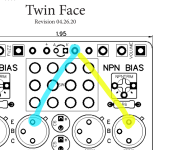
Measuring voltage between the negative connection point on the PCB and the emitter on NPN2 shows 0.71v regardless of what the trim pot is adjusted to.
Measuring voltage between the negative connection point on the PCB and the emitter on PNP2 shows 0.75v regardless of what the trim pot is adjusted to.
These values seem way off from the ideal 4.5v, any ideas on what I should do from here?
Here's a screengrab of the test points I'm using in my attempts to bias the circuit: blue line is showing 0.75v and the yellow line shows 0.71v no matter where I adjust the two trims on the PCB.

