PCB RFC - Grindhaus Fuzz

leadfoot

Well-known member
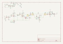
After seeing the DOD Grindhaus Fuzz show up in the wish list section and reading up on it and figured I'd make a version of it.

I based it off of the Hype Fuzz from FuzzDog, tossed in the Big Muff tone stack (with the ability to bypass), and then the make up boost as seen in the DOD Grindhaus documentation.

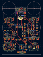
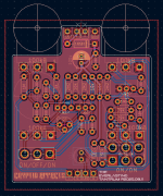
I've attached the schematic circuit and the pcb routing and would like feedback on how to make it better. I'll be using a ground pour on front and back to handle the grounds. When it is all done, I'm using the mad bean suggested trace sizes for power and signal.

I'll be happy to share the gerbers so others can make it as well.

Thanks!

Schematic:
Grindhaus Fuzz - Schematic.jpg

PCB:

grindhaus-fuzz-pcb.png
 
Nice! I'm no expert so take all of this with a grain of salt. I also mostly route SMD layouts but I think most of the advice will hold.
Some specific feedback:

- Kicad's default track width is soooo smol. Even with SMD components I try to keep my trace width at 0.5mm instead of the default of 0.2mm.
- Try to avoid routing back side if you can. The less stuff you have on the back, the better your ground pour. I see a few places where you're routing on the back where you probably don't need to.
- Don't be afraid of routing longer than you need to, even routing around the outside edge to avoid crossing. I've found that it works well for me to route 9V or VREF around the outside edges since that often needs connections on various places around the board.
- For example pin2 of upper left pot could go all the way around the outside to output to avoid crossing thru the middle of the board.
- Likewise for the input.
- (And it almost feels like the input half and output half want to be switched, since the output comes in on the right but is controlled by the left pot, and vice-versa. Maybe not that big of a deal but then you potentially have more crosstalk)
- C11 is near, but not on, the center line of the board (eye twitch)
- For the silkscreening, it can be nice to have the component value visible after population so you don't need to bring a map when you are trying to diagnose something. But I do see a lot of through-hole designs like this.
 
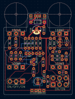
Looks good! The back will be a lot less broken up now. You might be able to spread the top row of resistors apart just a tad to get another trace or two between them rather than on the back. But maybe gilding the lily here.

One thing I notice that some people will point out is the 90 degree bends in the traces. If you were to get this reviewed on Reddit or something at least one person would have a stroke. The '45 degree angles only' is mostly a holdover from less refined etching processes, nowadays that is less of an issue, but it does violate 'best practices'. Also at higher frequency the 90-degree plus bends can actually cause more reflections/echos but I don't think it matters at audio frequencies. I still don't really know what to do about T/Y junctions myself though.

A tip I kind of recently learned in KiCad is the 'D' hotkey for 'drag'. You can grab a section of track and drag it around to make the angles more smooth. You can also set the router to 'push' so if you run into another track while dragging you push it instead of crossing it. There's also 'break track' which might only be in the right-click menu that you can use to create a joint in a track so you can drag the segment you just broke off. The 'D' key works on components, too. It will drag it along with tracks that are connected to the pads. Nice if you're moving things fairly small distances so you don't have to re-route. Like when you drag C11, Q1, Q2, Q3 and C5 to make them symmetric down the center line. (eye twitch) ;-)

Oh one more thing, don't forget to put some silkscreened text on there with your name/brand and a board revision number. Fact of life, you'll probably have more than one revision of this and when you dig it out of a drawer in a year you'll want to know if it's the one that works or not before you build it out. :-)
 
Thanks again! KiCAD is definitely a learning curve from EasyEDA where I used to make my PCBs. I'll probably clean up the routes again cause I'm not super happy with the ground pours and the way Q4 worked out.

I'll throw a name on everything along with a revision.. I'm thinking "The Everlasting Tantrum" is a good name for the pcb.
 
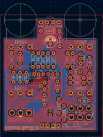
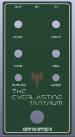
And here is the near final revision. I'm going to make sure the spacing is 2.54mm between pads on top and bottom, create a sweet faceplate then send them off to JLPCB and see what we get. :)

And again, if you see anything that looks suspicious, let me know so I can improve it.

grindhaus-fuzz-r2025.09.10.png
 
And again, if you see anything that looks suspicious, let me know so I can improve it.
Looks pretty good. A few small things.

- There's nothing stopping you from rotating q4 so it's oriented the same way as the other transistors. Just connect the middle pin to C9 first. It will be slightly cleaner than what you have. I'd prob rotate q3 as well.

All the solid blocks that look blue will not have a ground plane on the front, It'll look a bit gross and I think has more noise potential. I'll usually flip a few traces to the back of the board to fill those in - or nudge the traces/components slightly. Eg your spdt to 100n can go on the back. Same with the lower trace from the 100u cap, or the long trace from C9.

I'll usually do a pass to see if swapping the order of any lined up components will reduce trace length. In your case the 10k and 2m2 transistor can be swapped and the vertical pad traces will get shorter for each. I'd probably space that whole section out a bit and then you can run the blue trace to the right of the 1k resistor and avoid two crossovers.

Lastly, the control layout is slightly odd. In particular I think you can push the switches up a bit to get more even spacing on the front of the board. Because the pots are offset vertically it can be hard to judge this. Iirc you can see the pyrocumulus as an example.

Make sure you run the error checker after all your changes are done.
 
Looks pretty good. A few small things.

- There's nothing stopping you from rotating q4 so it's oriented the same way as the other transistors. Just connect the middle pin to C9 first. It will be slightly cleaner than what you have. I'd prob rotate q3 as well.
Agreed, I was working on that after posting this last image. It's a never ending improvement cycle...

All the solid blocks that look blue will not have a ground plane on the front, It'll look a bit gross and I think has more noise potential. I'll usually flip a few traces to the back of the board to fill those in - or nudge the traces/components slightly. Eg your spdt to 100n can go on the back. Same with the lower trace from the 100u cap, or the long trace from C9.
Good idea, I'll take a look at moving those around and get some more ground plane fill.

I'll usually do a pass to see if swapping the order of any lined up components will reduce trace length. In your case the 10k and 2m2 transistor can be swapped and the vertical pad traces will get shorter for each. I'd probably space that whole section out a bit and then you can run the blue trace to the right of the 1k resistor and avoid two crossovers.
Nice! I'll definitely see about a bit more refinement in that area.

Lastly, the control layout is slightly odd. In particular I think you can push the switches up a bit to get more even spacing on the front of the board. Because the pots are offset vertically it can be hard to judge this. Iirc you can see the pyrocumulus as an example.
Can you explain this a bit more? I'm using the standard Pedal PCB spacing for potentiometers and switches: 33mm between pots horizontally and 25.4mm vertically. The switches should be falling in line with those measurements centering the switch at 25.4 vertically below the pot center control.

Make sure you run the error checker after all your changes are done.
Yup, I always do that.
 
Can you explain this a bit more?
I forgot the right PCB, it wasn't the pyrocumulus. The examples I had in mind are the Glyph and Trumpeter. PPCB boards rarely stack controls in 3 rows, but when switches are on the bottom in a third row, they're pressed close to the pots - close enough that I will put a piece of electrical tape between the two to prevent shorts.

Here's what that spacing looks like. Of course you can position controls as you like, but the vertical space available with 3 rows is fairly limited.
 
Back
Top