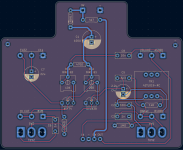
Did my best - the 4 remaining back layer traces are crossing.
Looks better! The ground plane is much less chopped up now.
I double checked and my stock (I have 50 or so) all fit the PPCB board footprints. My design uses .8mm holes will that be adequate?
... probably? The 1N5817 is usually a DO-41 package (not the smaller DO-35) and the datasheet claims ø 0.71mm legs. You might want ø 1mm hole size for easier insertion - it's not a huge deal since you're doing it by hand (and not machine placement) so the 0.8mm holes probably will work. But the larger holes also give more room for the solder to flow through from the back side.
I did this. Will passing directly under SW2 the way I did be a noise issue?
Probably not - it's relatively far away from the switch (what about 6mm or so?) with some ground plane in between so it should be fine even if that trace is bit noisy. You wouldn't want it running parallel (or on top of ) signal wires, but there's good separation here.
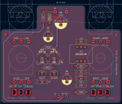
I completely re-arranged the right side of the board to address this. All pot footprints are now clear and the layout looks more organized.
Nice, looks good! Note that this isn't something you _have_ to do - and on most boards you probably won't be able to, they'll be too dense.
(unless you switch to SMD where you don't need to worry about what's on the other side in terms of leads poking thru the board). But it is something to keep in mind, it always annoys me when I've left just one of my pots with a bunch of through-hole pins behind it.
One last thing I noticed - you might think about moving the pins for the daughterboard south a little bit. If you get the north/south axis of your board right (e.g. take measurements, make it longer, etc) you can even use a tall pin header to connect the daughterboard to the PCB, but your header would have to be closer to the edge so the footswitch didn't collide. Screw soldering wires to things.
Also I might drop some ground vias near the far left - the ground connection there is fine on the front but is fenced off by the SW trace on the back, so some GND vias between the layers give that a more direct path. (although the GND pad of the FUZZ pot is reasonably close)