First PCB layout - How did I do? (updated version)

zakco

Member
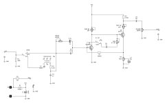
EDIT: I jumped the gun and there were some really significant wiring errors in my first attempt. I've attached updated versions here.

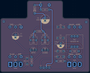
I've just finished my first PCB layout for my modified FF. It's not as tightly laid out or symmetrical as the commercial ones I've used, but I took my time and did my best! I followed the process from Pedal Division's video. I mostly used the footprints supplied by PD, but I had to make the one for the 42TL019-RC from scratch.

Is it suitable for fabrication?
Any feedback would be greatly appreciated, thanks!
 

Attachments

  • HANDFLOWER SCHEMATIC_261012.jpg
    HANDFLOWER SCHEMATIC_261012.jpg
    104.6 KB · Views: 16
  • HANDFLOWER PCB_261012.png
    HANDFLOWER PCB_261012.png
    182.8 KB · Views: 15
Last edited:
At first glance, the SW wiring is wrong. Power should go to CLR resistor -> LED -> SW pad
Yup. I just noticed a couple of other issues too...definitely jumped the gun! I just deleted the circuit from this post and will repost an updated version after I fix some pretty significant mistakes!
 
Ok...I think I've sorted out the wiring issues, there were a bunch!

At first glance, the SW wiring is wrong. Power should go to CLR resistor -> LED -> SW pad

I'm using PedalPCB 3PDT boards with LED, so the LED is not included on the main PCB and will be located as per my graphic design.

I've edited my first post with updated schematics and PCB layouts. Thanks for any input you can offer!
 
Looks pretty decent! Some feedback, all pretty minor, just best-practice stuff:

Mechanical
  • You might want to add 'Orthogonal Dimensions' on one of your user graphics layers to measure the dimensions between things, to make drilling your enclosures easier (more important when fitting to an existing enclosure). I like to use the potentiometer footprints that have silkscreen for where the shaft leaves the board so I can measure the distance between them, to make sure that the shaft is hitting the hole. (That didn't sound quite so filthy in my head but I'm leaving it)
  • Likewise, measure the width and height to make sure you're not super-squeezing this into a 125B. If you draw these dimensions all on one layer, they're easy to hide later.
Documentation
  • You should add silkscreen to the front and the back of your switches and pots -- since you'll be soldering them to back copper (probably) it's nice to have the silkscreen there so you don't screw it up and put them in backwards (ask me how I know). SW1/SW2 aren't labeled with what they are AFAICT and it sucks to have to open up KiCad with your laptop balanced on the corner of your electronics desk to figure out what they're for.
  • Label your switches ON/ON or ON/OFF/ON on the silkscreen -- same reason, so when you're digging thru your parts drawer you find the right ones.
  • Add a silkscreened board name and version -- top copper if you have room (and you do) since that'll be visible once it is in-situ. The version is important because I hate to tell you this but you'll likely have V2 of this board
Routing
  • Your top/bottom copper selection seems pretty arbitrary. IMO you should try to get all of your traces on one layer if you can and leave the other layer as un-cut as possible -- better ground plane that way. You don't have to snake vias up and down or anything, but you could put any non-crossing trace all on one layer which leaves a more unbroken ground plane on the other side. (And speaking of vias, you can add a couple ground vias too -- for through-hole it's less important since you have natural vias created by the through-holes - but you might want one at every 1cm corner or something)
  • Your 1n5817 probably wants a slightly bigger footprint than that. The ones I have are chonky and the leads are pretty thick, you might find yourself forcing those holes a little bit.
  • You could probably wrap the whole SW trace around the left side of the board if you wanted to, it's very near the input and shouldn't be too noisy - it gets rid of the big north-south cut.
  • Maybe not a huge deal but your range pot is gonna have a bunch of pins sticking out behind it and the other pots are not - so that one will be pushed away from the board a bit. I do most of my stuff as SMD and try not to put through-holes behind where the pots will lay against the board. It isn't a dealbreaker or anything but it's something to think about.
 
Looks pretty decent! Some feedback, all pretty minor, just best-practice stuff:
Well, that makes me happy, it's been a steep learning curve! And thank you so much for spending so much time on a detailed point by point reply, it's very helpful and I really appreciate it! This forum is awesome.

* You might want to add 'Orthogonal Dimensions' on one of your user graphics layers to measure the dimensions between things

I have this, but had it hidden for this screenshot to make it more legible. I've included in in the new version

* Likewise, measure the width and height to make sure you're not super-squeezing this into a 125B. If you draw these dimensions all on one layer, they're easy to hide later.

It’s a 1590BB enclosure and I have a graphic representation of that (was also hidden) that I used for determining the overall PCB dimensions. I have double checked and the 3PDT board will fit nicely and the bottom. The Pedal Division footprints I used came with 3D models, so I have also verified the jacks and pots that way. Everything seems to fit nicely.


* You should add silkscreen to the front and the back of your switches and pots
Great idea - done.
* Label your switches ON/ON or ON/OFF/ON on the silkscreen -- same reason, so when you're digging thru your parts drawer you find the right ones.
Check.
* Add a silkscreened board name and version -- top copper if you have room (and you do) since that'll be visible once it is in-situ. The version is important because I hate to tell you this but you'll likely have V2 of this board
Roger that.
* Your top/bottom copper selection seems pretty arbitrary. IMO you should try to get all of your traces on one layer if you can and leave the other layer as un-cut as possible
Did my best - the 4 remaining back layer traces are crossing.
* Your 1n5817 probably wants a slightly bigger footprint than that.
I double checked and my stock (I have 50 or so) all fit the PPCB board footprints. My design uses .8mm holes will that be adequate?
* You could probably wrap the whole SW trace around the left side of the board if you wanted to, it's very near the input and shouldn't be too noisy - it gets rid of the big north-south cut.
I did this. Will passing directly under SW2 the way I did be a noise issue?
* Maybe not a huge deal but your range pot is gonna have a bunch of pins sticking out behind it and the other pots are not
I completely re-arranged the right side of the board to address this. All pot footprints are now clear and the layout looks more organized.

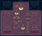
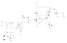
Here are updated images. How does this new version look?
 

Attachments

  • HANDFLOWER FUZZ_PCB_261013.png
    HANDFLOWER FUZZ_PCB_261013.png
    119.9 KB · Views: 15
  • HANDFLOWER SCHEMATIC_261013.jpg
    HANDFLOWER SCHEMATIC_261013.jpg
    101.9 KB · Views: 15
Did my best - the 4 remaining back layer traces are crossing.

Looks better! The ground plane is much less chopped up now.

I double checked and my stock (I have 50 or so) all fit the PPCB board footprints. My design uses .8mm holes will that be adequate?

... probably? The 1N5817 is usually a DO-41 package (not the smaller DO-35) and the datasheet claims ø 0.71mm legs. You might want ø 1mm hole size for easier insertion - it's not a huge deal since you're doing it by hand (and not machine placement) so the 0.8mm holes probably will work. But the larger holes also give more room for the solder to flow through from the back side.

I did this. Will passing directly under SW2 the way I did be a noise issue?

Probably not - it's relatively far away from the switch (what about 6mm or so?) with some ground plane in between so it should be fine even if that trace is bit noisy. You wouldn't want it running parallel (or on top of ) signal wires, but there's good separation here.


I completely re-arranged the right side of the board to address this. All pot footprints are now clear and the layout looks more organized.

Nice, looks good! Note that this isn't something you _have_ to do - and on most boards you probably won't be able to, they'll be too dense.
(unless you switch to SMD where you don't need to worry about what's on the other side in terms of leads poking thru the board). But it is something to keep in mind, it always annoys me when I've left just one of my pots with a bunch of through-hole pins behind it.

One last thing I noticed - you might think about moving the pins for the daughterboard south a little bit. If you get the north/south axis of your board right (e.g. take measurements, make it longer, etc) you can even use a tall pin header to connect the daughterboard to the PCB, but your header would have to be closer to the edge so the footswitch didn't collide. Screw soldering wires to things.

Also I might drop some ground vias near the far left - the ground connection there is fine on the front but is fenced off by the SW trace on the back, so some GND vias between the layers give that a more direct path. (although the GND pad of the FUZZ pot is reasonably close)

 
The 1N5817 is usually a DO-41 package (not the smaller DO-35) and the datasheet claims ø 0.71mm legs. You might want ø 1mm hole size for easier insertion
Ok, will do.

Probably not - it's relatively far away from the switch (what about 6mm or so?)

It’s 3mm from the edge of the pad to the edge of the trace -roughly 5 mm from the center of the switch pins.

One last thing I noticed - you might think about moving the pins for the daughterboard south a little bit…. <snip>…Screw soldering wires to things.

Indeed. I’ll consider this.
Also I might drop some ground vias near the far left - the ground connection there is fine on the front but is fenced off by the SW trace on the back, so some GND vias between the layers give that a more direct path. (although the GND pad of the FUZZ pot is reasonably close)

I’m not entirely clear as to where exactly you mean…in the bottom left corner between the switch and the SW trace?
 
I’m not entirely clear as to where exactly you mean…in the bottom left corner between the switch and the SW trace?

On the left side, where I assume the ground from the jack comes in - that piece of copper gets turned into a bit of an island on the back side.
Think of the traces like walls of a maze -- the current has to move along the path the maze makes to get wherever they're going. Sometimes you can arrange the walls in a way that there's no escape. Adding vias is like adding ladders to a second level of the maze that has different walls. A perfect unbroken ground plane is a maze with no walls.
 
EDIT: I solved my problem below, but I'll leave it here in case someone else is having the same problem.

One thing I'm stuck on though, is that I'm trying to add a couple of test points for setting collector bias on Q1 and Q2. The SMD test pads from Kicad's library don't show up in the PCB editor after updating from the schematic. What is the correct way to add a test point to the front copper layer that is connected to the collector pad?

The reason is that the test pads have no default footprint. One must added manually. Once I did that, they show up as expected.
 
Last edited:
On the left side, where I assume the ground from the jack comes in - that piece of copper gets turned into a bit of an island on the back side.
Think of the traces like walls of a maze -- the current has to move along the path the maze makes to get wherever they're going. Sometimes you can arrange the walls in a way that there's no escape. Adding vias is like adding ladders to a second level of the maze that has different walls. A perfect unbroken ground plane is a maze with no walls.
Got it. I've added a few elsewhere as well, where there were small islands.

Turns out I wired both the volume pot and Range pot backwards...sheesh!
So after fixing that, I decided to change the both transistor footprints to TO-5, which of course meant moving a bunch of stuff, which led to moving other stuff, and well...jeez...I swear I'll never be finished this thing! :LOL:

Having said that, maybe I'm done? How does the latest version look to you?
 
Last edited:
Back
Top