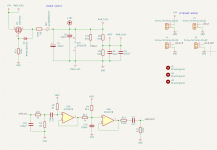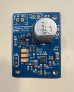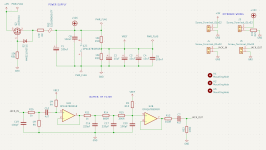
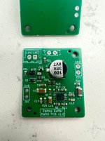
Here's my submission for most boring build of 2026: an always-on unity gain buffer. It's... delightfully unremarkable! The opamp is an opa1678. Since that's a dual opamp, it's basically a double-buffer with a little bit of high-frequency filtering between active stages. (And the opa1678 has some inbuilt RF protections.)
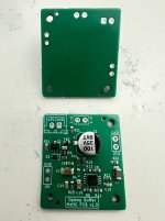
The back side is a fully contiguous ground plane!
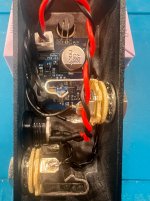
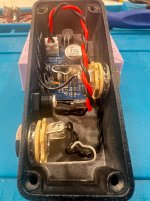
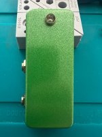
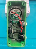
The only interesting part was the mechanical aspect: for my first attempt, I just eye-balled the drill holes, and ended up with something that didn't work.
So I took a little time to measure on the second attempt, to ensure I'd end up with something that can actually be assembled.
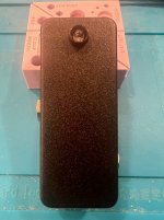
This is my first 1590A build, and even though the PCB itself is tiny, the mechanical/fitment aspects are really challenging!
The intent is for this to be mounted underneath my pedalboard.
Edit: See post #16 below for an update v1.0 buid.
The back side is a fully contiguous ground plane!
The only interesting part was the mechanical aspect: for my first attempt, I just eye-balled the drill holes, and ended up with something that didn't work.
So I took a little time to measure on the second attempt, to ensure I'd end up with something that can actually be assembled.
This is my first 1590A build, and even though the PCB itself is tiny, the mechanical/fitment aspects are really challenging!
The intent is for this to be mounted underneath my pedalboard.
Edit: See post #16 below for an update v1.0 buid.
Attachments
Last edited: