also, i'm sure this has been covered extensively elsewhere (so please feel free to just drop a link), but what is the advantage of using a relay over, say, a CD4053?
CD4053 is not a perfect switch. One has to consider on-resistance, off isolation, linearity, crosstalk and charge injection. They can and have been used successfully when applied correctly. They are more reliable than relays, although a relay does not significantly impact the reliability of a guitar pedal. Analog switches require more parts than a relay solution because they do not support true bypass. What Boss & Ibanez do with JFET switches could be done with a CD4053 or another CMOS switch.
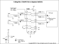
okay, so this is my existing bypass switching scheme, with a second tactile (small slide) switch to choose between true bypass or using the circuit's existing input buffer for a buffered bypass:
the 3PDT switch that i had previously been using has been replaced by the relay switches, with the cd40106 relay controller and power section off the page. what i was wondering about was your suggestion of using two of the other 40106 converters to drive another MOSFET switch, to cut the signal after the buffer. as it stands, in buffered bypass mode the signal goes through the whole pedal and only gets cut at the output. i'd ideally like to change this for two reasons: 1) i'm currently working on two relatively high-gain fuzz pedals with clipping LEDs that are incorporated into the pedal artwork, and i want them to stop lighting up when the pedal is in buffered bypassed mode; and 2) i've heard it's generally good practice to switch pedals off at the input, in order to keep noise to a minimum, especially in high-gain pedals.
so i attached a second set of what i assumed were the relevant switching parts of the 40106 to the momentary switch -- i assume the two capacitors are for debouncing the momentary switch, so they don't need to be copied again, but the 100k and two 10k resistors are part of the switching circuit. so that would look like this:
(edit: oops! r9 should be 10k, not 100k)
please let me know if i've made any other mistakes here.
incorporating that into the bypass switching circuit i thought would look like this (part of the power section is cut off in the screenshot because it isn't really relevant to the discussion):
but then i realized that although the MOSFET is isolated from the input jack by the input buffer, without an output buffer it's potentially exposed to the outside world through the output jack. so that means i could use the second half of the TL072 as an output buffer, and not have a buffered VREF, or else i could place the circuit disconnect switch one stage deeper into the circuit, which means sending the switch signal off the i/o board to drive a MOSFET on the main circuit board. which isn't a deal breaker either.
anyway please let me know if i've made any mistakes in my circuit or my thinking.
")