Custom microcontroller-based relay bypass - update - v2.0 board

MattG

Well-known member
Build Rating
5.00 star(s)
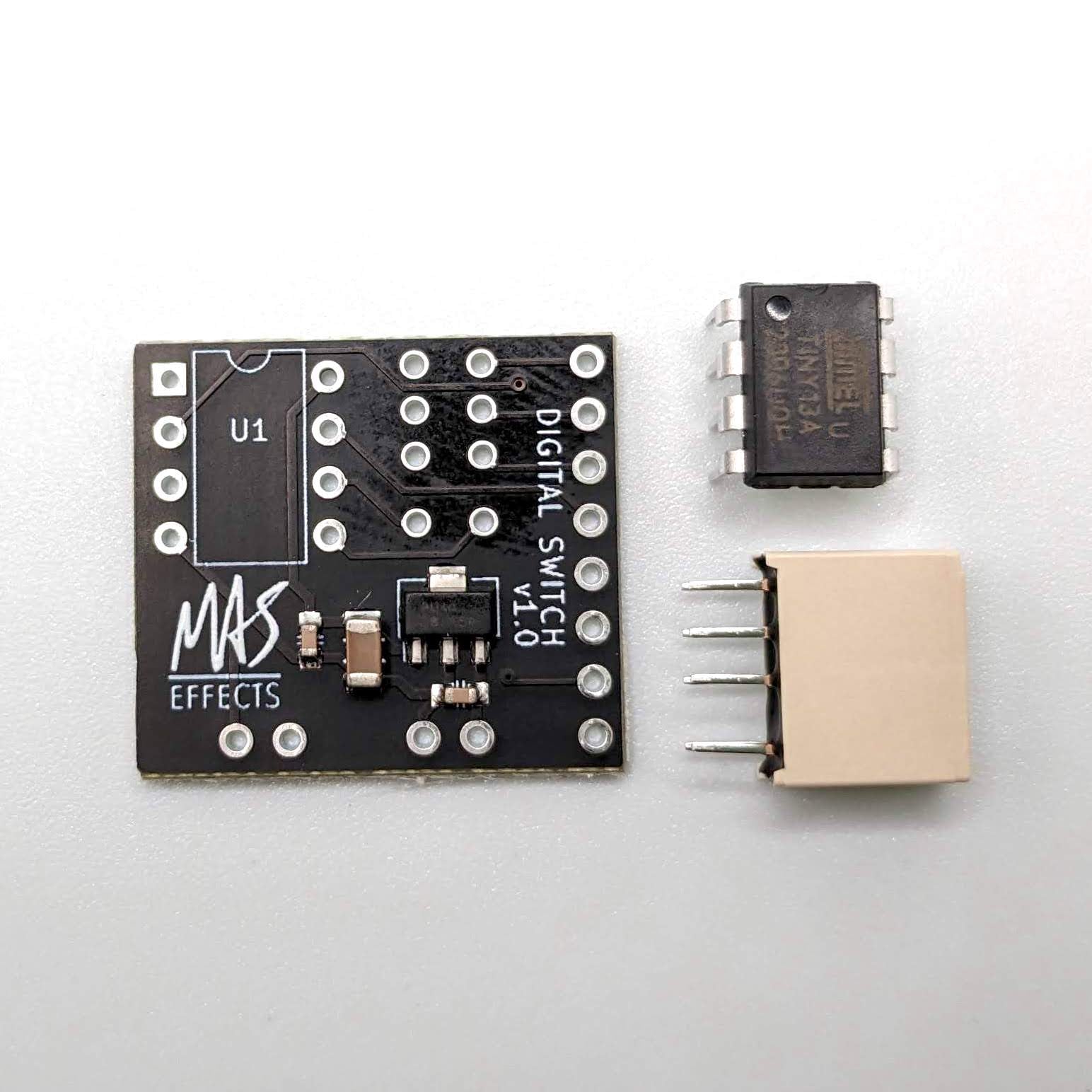
Something I've been slowly working on for a while now: microcontroller-based relay bypass. It's become a mini-obsession, I want the "luxury feel" of a momentary switch, the increased reliability of a relay (compared to the 3PDT mechanical switch), and the lowest possible power consumption. I also wanted to have a central reference implementation for readily available microcontrollers and a mating hardware circuit. I'm finally at a point where I feel I have a good start.

What I've created is a generic interface for the microcontroller code, and implementations for the ATtiny13, ATtiny85, PIC12F675 and PIC10F320 microcontrollers. I created a v1.0 PCB for the AVR (ATtiny) MCUs. The same circuit on a breadboard works with the PIC devices (the pinouts are different on the PIC and AVR MCUs, so I'd need a bunch of jumpers to have a single board). The "innovation" (if I can be so self-generous) here is that I enable a pin-change interrupt so I can put the MCR to sleep when it's not doing anything. The interrupt will wake it from sleep, it changes state, then goes back to sleep. These MCUs really sip current in sleep mode.

The code is open source (MIT license).

This v1.0 PCB drives the relay coil directly from the MCU. The AVR chips have protections that make this OK. I couldn't find detailed docs on the PIC microcontrollers' IO pin protections. "It works on the breadboard" doesn't necessarily mean it's a long-term, robust design. So the next revision will use transistors to drive the relay coil, and have explicit flyback protection diodes. Arguably overkill for the AVR chips, but a more general design.

I updated three of my builds with this relay bypass:
Below are pics of the updated builds. I also included a photo of my PCB next to the PedalPCB Basic Relay Bypass. Nearly the same dimensions (though, as I said, this is v1.0, v2.0 will be slightly bigger).

I'm pretty happy with this. The Snozzberry and Tellurian Drive are daily-use pedals for me. So far no issues! I also just built a new pedal (build report coming soon) that uses this relay bypass.

If anybody is interested in helping with testing, I'm willing to send out a board or two with a pre-programmed MCU. PM me if interested.
 

Attachments

  • IMG_7225.jpg
    IMG_7225.jpg
    470.9 KB · Views: 84
  • IMG_7233.jpg
    IMG_7233.jpg
    553.5 KB · Views: 82
  • IMG_7232.jpg
    IMG_7232.jpg
    564.8 KB · Views: 73
  • IMG_7231.jpg
    IMG_7231.jpg
    600.9 KB · Views: 72
  • IMG_7230.jpg
    IMG_7230.jpg
    542.3 KB · Views: 63
  • IMG_7229.jpg
    IMG_7229.jpg
    558.1 KB · Views: 66
  • IMG_7228.jpg
    IMG_7228.jpg
    590.5 KB · Views: 58
  • IMG_7227.jpg
    IMG_7227.jpg
    768.8 KB · Views: 61
  • IMG_7226.jpg
    IMG_7226.jpg
    552.4 KB · Views: 82
This is super cool! I just got into flashing my own MCUs using the open source Mas Effects repo, and I will probably always use them instead of 3PDT breakouts going forward. I'm glad there's another option now, and that it's MIT licensed! Props for contributing to the community in such a substantial way!
 
That's really nice. Opensource for the win!
I would recommend looking into using the same pin spacing for IO with the PCB for v2. It makes assembly so much easy if you can use pin headers, and it gives a stable platform. I was annoyed at the floating relay on my v1. Plus it plugs into a breadboard!
 
Thanks for sharing your work! I went down a similar soft-touch relay bypass rabbit hole a few years ago inspired by the CODA write-up and code.

I got frustrated by the unavailability of PIC chips during the height of covid and started making boards with the ability to use ATtiny or PIC (although since availability has changed I mostly just use ATtiny chips now). I can look up the schematic to share, but Here is an image & schematic of how I set a PCB to use either ATtiny or PIC12f675 (image is of the back of the PCB). For ATtiny I solder the two pads in the top row together and the left two pads in the middle row together, for PIC I solder the pads in the bottom row together and the right two pads in the middle row together. So it is really quick to switch a PCB to accept either type.


SCR-20230606-mgpv.png SCR-20230606-mvrb.png
 
Last edited:
That's really nice. Opensource for the win!
I would recommend looking into using the same pin spacing for IO with the PCB for v2. It makes assembly so much easy if you can use pin headers, and it gives a stable platform. I was annoyed at the floating relay on my v1. Plus it plugs into a breadboard!

To which IO pin spacing exactly are you referring?

Are you talking about the plated solder holes at the top of the board, for power, gnd, input/output jacks, and the four connections to the actual effect (in, out, sw, gnd)? If so, good eye! In their current state, those holes are kind of a wacky spacing/size. That's due to the fact that on a completely different bypass PCB I made months ago, I made those holes too small for normal hookup wire to fit through. I've since gone too far in the other direction! What you see now is over-big holes spaced too far apart. The v2.0 boards I'm waiting on indeed use a more standard 2.54mm pin header footprint, and the holes should be big enough for typical 22awg hookup wire. Assuming it turns out as expected, I'll actually make a revision 1.1 board that uses the sane wire holes.
 
I got frustrated by the unavailability of PIC chips during the height of covid and started making boards with the ability to use ATtiny or PIC (although since availability has changed I mostly just use ATtiny chips now). I can look up the schematic to share, but here is an image of how I set a PCB to use either ATtiny or PIC (image is of the back of the PCB). For ATtiny I solder the two pads in the top row together and the left two pads in the middle row together, for PIC I solder the pads in the bottom row together and the right two pads in the middle row together. So it is really quick to switch a PCB to accept either type.

If it's not too hard to find that schematic, I'd certainly be interested in taking a look at it!

It's funny you mention the PIC chip unavailability. When I first thought about doing this project, it was during the supply chain shenanigans. It actually discouraged me from starting this at the time. Supply chain issues was one of my main motivations for creating a generic interface that supports multiple MCUs out of the box, and (hopefully!) makes it easy to add support for others as well. Even without supply chain issues, I figured pricing and availability is likely different in different parts of the world.

Anyway, as far as the choose-your-own-MCU jumpers go: I assume you're talking about the pic12f675, since that's what CODA Effects site talks about. I also included support for the pic10f320, which has a different pinout from both the AVR and 12f675 parts. So I'd not only have to have 3-way jumpers for power and ground, but have to jumper IO pin(s). While I too personally prefer the AVR chips, that 10f320 is compelling because it's the cheapest, and also uses a tiny amount of power even without sleeping. (But I eventually plan to add support for a muting circuit, which requires a fifth IO pin, and the 10f320 has only four GPIO pins.)

But yes, MCU-agnostic PCB is absolutely a future goal!
 
If it's not too hard to find that schematic, I'd certainly be interested in taking a look at it!

Anyway, as far as the choose-your-own-MCU jumpers go: I assume you're talking about the pic12f675, since that's what CODA Effects site talks about. I also included support for the pic10f320, which has a different pinout from both the AVR and 12f675 parts. So I'd not only have to have 3-way jumpers for power and ground, but have to jumper IO pin(s). While I too personally prefer the AVR chips, that 10f320 is compelling because it's the cheapest, and also uses a tiny amount of power even without sleeping. (But I eventually plan to add support for a muting circuit, which requires a fifth IO pin, and the 10f320 has only four GPIO pins.)
I found and appended the relevant part of the schematic to my post above.

Very good point about the specific PIC, you are right - the PIC / ATtiny switching I show above is for PIC12f675. Things are going to get more difficult with more flexibility in PIC choice, I had not appreciated that.

I have been finding ATtiny13A SMDs reliability from mouser for <$0.75 each, which for the small numbers I buy at a time is cheap enough that I just get them and have stopped shopping around. It is nuts to me that they can make and sell microcontrollers for so little now.
 
I did the same thing with the same PIC10F320. One thing to mention is there is also a PIC10F322 version with double the flash size. If you want to add it as a supported MCU.

Do you program the MCUs out of the circuit? It would be nice to have some unified programming interface such as tag-connect eventually.
 
I just received my v2.0 boards yesterday. I built the first one up and installed it in my Tellurian. Works great!

The code microcontroller code for the v1.0 and v2.0 boards is exactly the same. The v2.0 board is slightly larger, but decouples the MCU from driving the relay coil with transistors (and the transistors are protected with flyback diodes). It's a more generic design where I don't have to worry about the MCU having enough current source/sinking ability for the relay coil, and also don't have to worry about the MCU having protection diodes for the coil kickback. It also runs at 3.3v volts and uses a two-coil latching relay (Kemet EC2-3TNU).

(Side note: keen eyes will notice the nasty mess of flux residue on the clipping diode area of the Tellurian build. That is the result of me soldering in different diodes. I really should have installed sockets! Frankly I'm surprised it still works, the board definitely won't tolerate another round of soldering. I also put a 510k resistor across the drive pot, turning it into a poor man's 250k pot. I was trying for more "edge of breakup" sweep of the pot, but this didn't really achieve that.)

Anyway, once again, if anyone is interested in adding my relay bypass to your build, PM me, I'd appreciate some more in-the-field testing.

Edit: forgot to post the pics!
 

Attachments

  • IMG_7308.jpg
    IMG_7308.jpg
    461 KB · Views: 39
  • IMG_7307.jpg
    IMG_7307.jpg
    452.1 KB · Views: 37
I just received my v2.0 boards yesterday. I built the first one up and installed it in my Tellurian. Works great!

The code microcontroller code for the v1.0 and v2.0 boards is exactly the same. The v2.0 board is slightly larger, but decouples the MCU from driving the relay coil with transistors (and the transistors are protected with flyback diodes). It's a more generic design where I don't have to worry about the MCU having enough current source/sinking ability for the relay coil, and also don't have to worry about the MCU having protection diodes for the coil kickback. It also runs at 3.3v volts and uses a two-coil latching relay (Kemet EC2-3TNU).

(Side note: keen eyes will notice the nasty mess of flux residue on the clipping diode area of the Tellurian build. That is the result of me soldering in different diodes. I really should have installed sockets! Frankly I'm surprised it still works, the board definitely won't tolerate another round of soldering. I also put a 510k resistor across the drive pot, turning it into a poor man's 250k pot. I was trying for more "edge of breakup" sweep of the pot, but this didn't really achieve that.)

Anyway, once again, if anyone is interested in adding my relay bypass to your build, PM me, I'd appreciate some more in-the-field testing.

Edit: forgot to post the pics!
There's a lot of great stuff there. Awesome stuff. I love the design choices!
 
I just posted two build reports: Celestial Drive and Heliodor where I used the latest revision of my board, v3.0. Changes for this board:
  • Custom footprint that supports two different relays (Kemet EC2-3TNU or Panasonic TQ2-L2-3V)
  • Designed for PIC10F320 or PIC10F322 microcontrollers
  • Added a "board power" solder hole for compatibility with AionFX boards
  • Cosmetic improvements to the silkscreen

It's only been a couple days, but so far so good. The actual MCU code is unchanged since I tagged it "v0.1" a couple months ago. Previously my PCBs were designed around the ATtiny MCUs, and I'd only tested the PIC MCUs on a breadboard. Nice to see them working as expected in their actual intended application!

I actually made this v3.0 board a four-layer board. Which is expensive and overkill for this purpose. But it made the routing easier! I've since tweaked the routing to be clean on a two-layer board. That will be PCB v4.0 and will also go back to being for the ATtiny. After that, I'll likely do a surface-mount version (for maximum space-savings).

I still have lots of boards and extra pre-programmed MCUs I'm willing to send out to anyone who wants them. (I know there's one of you out there waiting on a shipment, hoping to get to that this weekend!)
 
Last edited:
For folks who use Arduino IDE with their ATtiny and have some arbitrary soft-touch board, I have posted my arduino sketch file for soft touch here:

It mimics all the features I know of in the various versions of soft touch boards. The obvious differences between boards is pin assignment. I wish I had seen this thread before I forged out on my own. :)

It has build switches to choose the platform and desired features. At the moment, it can be targeted toward the Sparkfun tiny programmer (for development and debug), Digispark, PedalPCB IRB, MAS effect with optocoupler mute, MAS effect generic and, added today, Matt's board. :) Are there others worth adding? Is an arduino file useful to anyone?

My sketch file started from the MAS effect code, which is also open source. Very cool stuff.

Can be configured for latching or non latching relays. Non latching is mainly for use in situations where a relay is not what is being controlled. I originally dove into this to make a soft-touch enable for my TPA3118 power amp pedal over here:

It can toggle between modes by holding the foot switch at power on. Or, you can force the power on state with a build switch.
The 3 boot modes are Bypassed, Engaged or Remember the state of previous power down.
If the control signal feature is enabled then the third state is "honor the incoming control signal" instead of remembering state.

It can do the "temporary toggle state" when holding the switch for more than a half second.

Can use NO or NC momentary foot switch, if you happen to have ordered a pile of NC by accident.

Uses software debouncing, so no cap is needed across the switch lines.

Can include a power-on time delay during which it remains bypassed. This was also for my power amp pedal so that the power amp remains muted for 5 seconds while everything is stabilizing.

Has a level sensitive mode that is engaged with the switch pressed and bypassed unpressed. This is for cases when the module doesn't have a switch but is monitoring some other signal to know if it should be engaged or not. See this thread for example use:

Supports the second LED of the MAS effect generic board.

The control signal support can be used on other boards. For example, the mute signal or second LED of the MAS boards can become a control signal instead just by configuring the build switches... The point of this is to make the general feature set portable to all the platforms since folks may have invested in different boards or want the alternate form factors. I happen to like the very tiny MAS boards...
 
By the way, if anyone is interested in trying out ATtiny85 programming in the cheapest possible way that can also be used with relay boards... Mouser has these olimex kits for $2.67. It works the same as a digispark with one key advantage: It comes with an ATtiny 8-pin dip and socket you can pull and move elsewhere, already loaded with micronucleus. So, you get the very easy cheap programming via micronucleus (no HW programmer needed) along with the ability to move the chip to another platform.

The down side... When first powered, micronucleus tries to connect to USB for 5 seconds, which toggles PB3 and PB4 furiously. That's bad if the chip is moved to a platform that has PB3 and PB4 hooked to something that is going to react badly to that. After 5 seconds, your code is launched if no USB connects.

The PedalPCB IRB has PB3 and PB4 used for the LED (driving the transistor) and the control line. So, it would be no big deal if those were going wild for 5 seconds. The generic MAS board uses PB3 and PB4 for LED2 and the foot switch, so again no big deal. Matt's board has PB3 going to a relay coil. I tried this on my MAS board for opto coupler, which has PB3 going to a relay coil and it works fine. The relay isn't freaking out or anything. Of course, it takes 5 seconds before it starts properly responding.

If you have a programmer, like the Sparkfun tiny programmer, then all this is moot. You've spent the $20 on a programmer, so no point having micronucleus on your tiny, unless you want the USB poking out the side of your pedal for reprogramming on the fly.
 
Last edited:
I re-wrote the core of my relay program to use a blocking state machine instead of the free-running timed states. Much easier code (for me anyway). The sketch file is posted here, replacing the previous one.

It now supports the temporary switch feature (hold the switch longer than 500ms to revert state when released) and this feature works along side the multi-module control feature. So, you can temporarily engage one module and, when released, if another module was dis-engaged by the control line, it will go back to engaged.

Does anyone know of other features that should be added?

One thing to be aware of is that the code also slows the clock down to 125khz and assumes you are starting with default fuses: 8Mhz clock with clock divider set to 8 to get 1Mhz. It's very important to have all the clock frequency stuff set properly and known, or none of this works right. And, once you program the chip to run at slow clock speed, your programmer must have a 100k pull-down resistor on the reset pin so the code doesn't start up and cut the clock speed. The programmer won't be able to program the chip if the clock speed has been reduced below 1Mhz by the running code.

The structure of the code is very simple with non-overlapping, blocking states...

The loop() function is the idle state waiting for the switch to be pressed or the control line to be asserted.
If the switch is pressed, jump to the switchPressed() function. switchPressed() will not return until the switch is released.​
If the control signal is active, jump to the ctrlState() function. ctrlState() will not return until the control line is not active.​

switchPressed(): This is a blocking state.
Assert the control line if about to change to engaged state.​
Toggle the relay.​
Wait for the switch to be released...​
Deassert the control line.​
If the switch was held longer than 500ms: toggle the relay again.​
Return to loop().​

ctrlState(): This is the other blocking state.
If engaged, change relay state to bypassed.​
Wait for the control signal to go inactive...​
If the control signal was longer than 500ms, return the relay to the state it was initially.​
Return to loop().​

Quick Edit: Changed it to interrupt driven and sleeps waiting for a signal. The tiny is drawing about 700uA most of the time now. LEDs dominate the power draw.

Another quick edit. Found with a simulator that the code was not sleeping and that delay() doesn't work inside interrupts. Fix both and posted the new file (10/24/2023). Also made my simulation project public. Pretty nifty tool:
 
Last edited:
Back
Top