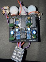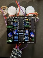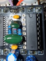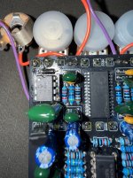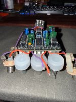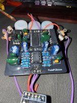
Hey all! I’m scratching my head over here. Slowly but surely I’m learning what all these little doodads do in these pedals and I’ve gotten fairly good at troubleshooting my builds but this one has me stumped.
Built a deflector, had the FV-1 soldered for me but when you turn it on, there’s almost a 50% volume drop, almost exactly too, hooked up a signal generator to it and scoped the output and it was almost exactly half of the input when the pedal is turned on, also the LED is really dull.
I’ve taken some decent notes on what I’ve done as far as troubleshooting and took some halfway decent pictures. Hopefully someone can help me figure this out!!
# Deflector Reverb (PedalPCB) Troubleshooting Summary
**Symptom:** Volume drop when effect is engaged
## Power Rail Checks (all measured with 9V DC supply, referenced to ground)
| Test Point | Expected | Measured | Status |
| D100 (1N5817) drop | ~0.2 to 0.3V | 0.31V (9.26V in, 8.95V out) | Good |
| IC5 (L78L33) Pin 3 input | ~8.95V | 8.95V | Good |
| IC5 Pin 2 GND | 0V | 0V | Good |
| IC5 Pin 1 output | 3.3V | 3.3V | Good |
| IC1 (TL072) Pin 8 V+ | ~9V | 8.95V | Good |
| IC1 Pin 4 V- | 0V | 0V | Good |
| IC2 (SPIN FV-1) Pin 14 | 3.3V | 3.28V | Good |
| IC2 Pin 15 | 3.3V | 3.28V | Good |
| IC2 Pin 27 (VREF) | ~1.65V | 1.68V | Good |
| IC4 (CD4049UB) Pin 1 VDD | ? | 3.20V | See notes |
| IC4 Pin 8 VSS | 0V | 0V | Good |
All rails are clean. Every IC is receiving expected supply voltage. The 3.3V regulator is solid and the FV-1 VREF is correct.
**IC4 (CD4049UB) VDD reads 3.20V.** Initially suspected this should be 9V, but the CD4049 may be **intentionally powered from the 3.3V rail** by design. This is unconfirmed and needs clarification from someone familiar with the PCB layout.
## Continuity Checks (power OFF)
| From | To | Result | Notes |
| IC4 Pin 1 leg | IC4 Pin 1 solder pad | Beep | Socket and chip connection good |
| IC4 Pin 1 | IC4 Pin 2 | No beep | No solder bridge between adjacent pins |
| IC4 Pin 1 | IC1 Pin 8 (9V rail) | No beep | CD4049 VDD is NOT on the 9V bus |
| IC4 Pin 1 | IC5 Pin 1 (3.3V output) | No beep | Not directly connected to 3.3V regulator output either |
| IC4 Pin 1 | Duration pot left lug | Beep | Trace confirmed from IC4 VDD to Duration pot |
| Duration pot left lug | Duration pot middle lug | Beep | Normal wiper connection |
| Duration pot right lug | IC1 Pin 8 (9V rail) | No beep | Right lug is not on 9V bus |
| Duration pot right lug | IC4 Pin 1 | No beep | |
| Duration pot right lug | IC3 Pins 1, 2, 3, 5, 8 | Beep | Right lug appears to be on the 3.3V net (EEPROM address pins + VCC)
## Summary and Open Questions
1. All power rails check out clean. FV-1 has good 3.3V power and correct VREF bias.
2. The CD4049UB (IC4) VDD measures 3.20V. We could not confirm via continuity whether this is by design or a fault. IC4 Pin 1 has no direct continuity to the 9V rail (IC1 Pin 8) or the 3.3V regulator output (IC5 Pin 1), but does trace through the Duration pot to the 3.3V EEPROM net.
3. **Key question for the forum: Is IC4 (CD4049UB) supposed to be powered from 3.3V or 9V on this board?** If 9V, there's a routing issue. If 3.3V, the volume drop is elsewhere and we need to move on to signal tracing.
4. No signal tracing done yet. Next step would be injecting a test signal from the oscilloscope cal output and measuring levels at each stage of the signal path.
5. No solder bridges detected between IC4 pins 1 and 2. All solder joints on IC4 socket appear solid.

Built a deflector, had the FV-1 soldered for me but when you turn it on, there’s almost a 50% volume drop, almost exactly too, hooked up a signal generator to it and scoped the output and it was almost exactly half of the input when the pedal is turned on, also the LED is really dull.
I’ve taken some decent notes on what I’ve done as far as troubleshooting and took some halfway decent pictures. Hopefully someone can help me figure this out!!
# Deflector Reverb (PedalPCB) Troubleshooting Summary
**Symptom:** Volume drop when effect is engaged
## Power Rail Checks (all measured with 9V DC supply, referenced to ground)
| Test Point | Expected | Measured | Status |
| D100 (1N5817) drop | ~0.2 to 0.3V | 0.31V (9.26V in, 8.95V out) |
Good || IC5 (L78L33) Pin 3 input | ~8.95V | 8.95V |
Good || IC5 Pin 2 GND | 0V | 0V |
Good || IC5 Pin 1 output | 3.3V | 3.3V |
Good || IC1 (TL072) Pin 8 V+ | ~9V | 8.95V |
Good || IC1 Pin 4 V- | 0V | 0V |
Good || IC2 (SPIN FV-1) Pin 14 | 3.3V | 3.28V |
Good || IC2 Pin 15 | 3.3V | 3.28V |
Good || IC2 Pin 27 (VREF) | ~1.65V | 1.68V |
Good || IC4 (CD4049UB) Pin 1 VDD | ? | 3.20V |
See notes || IC4 Pin 8 VSS | 0V | 0V |
Good |All rails are clean. Every IC is receiving expected supply voltage. The 3.3V regulator is solid and the FV-1 VREF is correct.
**IC4 (CD4049UB) VDD reads 3.20V.** Initially suspected this should be 9V, but the CD4049 may be **intentionally powered from the 3.3V rail** by design. This is unconfirmed and needs clarification from someone familiar with the PCB layout.
## Continuity Checks (power OFF)
| From | To | Result | Notes |
| IC4 Pin 1 leg | IC4 Pin 1 solder pad |
Beep | Socket and chip connection good || IC4 Pin 1 | IC4 Pin 2 | No beep | No solder bridge between adjacent pins |
| IC4 Pin 1 | IC1 Pin 8 (9V rail) | No beep | CD4049 VDD is NOT on the 9V bus |
| IC4 Pin 1 | IC5 Pin 1 (3.3V output) | No beep | Not directly connected to 3.3V regulator output either |
| IC4 Pin 1 | Duration pot left lug |
Beep | Trace confirmed from IC4 VDD to Duration pot || Duration pot left lug | Duration pot middle lug |
Beep | Normal wiper connection || Duration pot right lug | IC1 Pin 8 (9V rail) | No beep | Right lug is not on 9V bus |
| Duration pot right lug | IC4 Pin 1 | No beep | |
| Duration pot right lug | IC3 Pins 1, 2, 3, 5, 8 |
Beep | Right lug appears to be on the 3.3V net (EEPROM address pins + VCC) ## Summary and Open Questions
1. All power rails check out clean. FV-1 has good 3.3V power and correct VREF bias.
2. The CD4049UB (IC4) VDD measures 3.20V. We could not confirm via continuity whether this is by design or a fault. IC4 Pin 1 has no direct continuity to the 9V rail (IC1 Pin 8) or the 3.3V regulator output (IC5 Pin 1), but does trace through the Duration pot to the 3.3V EEPROM net.
3. **Key question for the forum: Is IC4 (CD4049UB) supposed to be powered from 3.3V or 9V on this board?** If 9V, there's a routing issue. If 3.3V, the volume drop is elsewhere and we need to move on to signal tracing.
4. No signal tracing done yet. Next step would be injecting a test signal from the oscilloscope cal output and measuring levels at each stage of the signal path.
5. No solder bridges detected between IC4 pins 1 and 2. All solder joints on IC4 socket appear solid.