So tonight I finished up a pedal based on a PCB of my own design. And when I powered it on... nothing! After some debugging, I found that one of the signal nets was shorted to ground. I narrowed it down to what I assumed were three possibly bad components. Fortunately, this part of the circuit is optional (it's a RF filter I wanted to test out). So I bypassed those components with a jumper wire, and it worked.
What I thought was interesting was, even after removing the suspect components, the net they shared (i.e. leads connected by the same trace) still showed continuity to ground.
So I got one of the bare PCBs and checked - same issue! In fact, all four of the unpopulated PCBs have the same issue - a net that should not have continuity to ground is in fact shorted to ground.
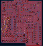
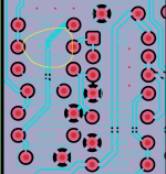
Here's a picture of the PCB with only the copper layers visible. This is a two layer board, with top (red) and bottom (blue) ground planes. The net I circled in yellow is the one that's shorted to ground. Kicad would throw a DRC error if I short two distinct grounds. And just now, I dropped a ground via on that trace, ran the DRC, and it indeed throws an error.
So this leads me to believe that either (1) the Gerbers Kicad generated are bad, or (2) JLCPCB had a manufacturing error.
Anyone ever experienced anything like this? @Robert, I believe you've ordered a lot of PCBs from JLC, has something like this ever happened to you?
Any further way I can be sure if it's a fabrication issue or a Kicad software issue?


