JFET Shootout

Same process as N-channel JFETs, just reverse the polarities, i.e. drain voltage is negative.

I should mention that my CCTT cannot test P-channel JFETs.
 
Last edited:
Just to add a small curiosity (a positive one, actually). I was looking through my J113 "collection" to find one for Q1 in the Viceroy that would bias up to 5V on the drain using the resistors from the schematic (10k drain and 1k8 source). The SMD ones I tested didn't bias right, VP too big. But in the end I found five through-hole J113 that do bias up to around 5V. I tested on the breadboard. My CCTT (it's simply named "Tester - T7") says they all have a VP of around -0.9V.

So, next I added the ROG tester from post #42 to the breadboard. And because I'm looking at J113 types I used a 1.75M test resistor as Chuck suggested in post #46. I wanted to see how my CCTT compares to the breadboard!

Below the whole shebang. DMM with new batteries, CCTT fully charged.

Code:
A few J113 transistors selected for Q1 in the Viceroy
 
IDSS in mA
VP in V

     Breadboard             CCTT                 Delta between Breadboard & CCTT
    IDSS    VP          IDSS   VP                IDSS    VP
Q1  6.86    -1.04       7.2    -0,945            0.34    0.095
Q2  7.40    -1.07       7.8    -0.985            0.40    0.085
Q3  7.18    -1.07       7.6    -0.978            0.42    0.092
Q4  7.34    -1.08       7.8    -0.990            0.46    0.090
Q5  7.11    -1.05       7.6    -0.965            0.49    0.085
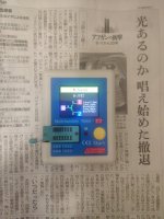
The CCTT cost me around 20 bucks a couple of years ago. Check mentioned in post #46 that he usually leaves out the resistor when testing and that because of this the measured VP would be a bit smaller (in magnitute!) than the actual one. One could make the argument that the CCTT obviously doesn't know what model of JFET it is currently testing. So it also cannot "put the right test resistor". So one could expect that the VP it outputs is also a bit on the smaller side.

Looking at the table that would actually make sense, as the CCTT measures the VP a little smaller in each case, and it does so in a pretty consistent way if you compare all the VPs measured between breadboard and CCTT. Same goes for IDSS, only there it's reversed, IDSS is measured a bit bigger by the CCTT.

I'm actually quite impressed, considering the CCTT only cost 20 bucks.
 
Last edited:
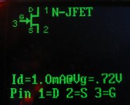
My CCTT does not measure either Vp or Idss and I'm not aware of any that do. Can you post a pic of the CCTT display when it's testing a JFET? Mine looks like this. The Id measurement is not Idss. The Vg measurement is not Vp. Is is simply the gate voltage at some arbitrary drain current.

J2902 CCTT.jpg


When you say "...the measured VP would be a bit smaller than the actual one." what we actually mean is that the Vp measurement is more negative when there is no resistor between source and gate because the drain current during the test is smaller (closer to zero).

It is always ok to trim the source or drain resistor to dial-in the bias. Just don't go more than ±25% from the nominal value, otherwise the gain and/or EQ might be impacted.
 
Hi Chuck,

Sure, pic attached.

tester-t7.jpg

In my opinion people in general mean magnitude when they say "higher VP" or "lower VP", like "2 is higher than 1", or "1 is smaller than 2", but they know that Vp for n-JFETs is negative, so mathematically "-2 is smaller than -1" and vice versa.

So when you said that without the resistor the VP reading is a little bit on the low side in post #46, I thought you meant the magnitude.

Anyway, moving on. I also added the delta to the table above.
 
Last edited:
There is some overlap in the specs of J201 & J202. So it's possible to sub the J202 in some circuits. J201s have a very broad Vp range. Some will not work in certain circuits that call for J201. The easiest way to know if a particular JFET will work in a given circuit is to try it.

I have a question for you: do you have any J202s?
 
There is some overlap in the specs of J201 & J202. So it's possible to sub the J202 in some circuits. J201s have a very broad Vp range. Some will not work in certain circuits that call for J201. The easiest way to know if a particular JFET will work in a given circuit is to try it.

I have a question for you: do you have any J202s?
I have some from DigiKey, yes. Also I've been trying out a preamp-style circuit made via JLCPCB using the surface-mount variety. I originally did the circuit with J201 but since I had a higher voltage (28V), and the higher Vp of the J202 would allow me to not have a voltage divider right at the input, I used those instead of J201. I had to bias differently, and the attenuation pads I had to adjust (a couple of gain stages and a tone stack), but what I found is that, perhaps because the parts in the same reel maybe came from the same wafer section, the Idss and Vp were a lot closer. I used the Fetzer-modified circuit for the stages, and found that pretty much the same standard Rd and Rs values could be used across all of these on each one I made (JLCPCB has a minimum of 5) on each board (I didn't populate Rd and Rs and put them in after measuring each stage).

I hope to post about this soon.
 
J202 are capable of higher gain (transconductance), but we have to run them at a higher drain current to achieve the higher gain. Higher drain current means we must either increase the power supply voltage or decrease the drain resistor. Decreasing the drain resistor reduces the gain, so that's not desirable. Since you're running at +28V, the J202 is a good JFET for the application. The other alternative to reducing the drain resistor is to replace the drain resistor with a μ-amp or SRPP configuration.
 
Back
Top