Chuck D. Bones
Circuit Wizard
In this chapter, we'll discuss the input characteristics of opamps and how to bias them.
In an ideal opamp,
1. The current flowing in or out of the input pins would be zero.
2. The voltage difference between the input pins would be zero when the opamp's output is halfway between the rails.
3. The opamp would work correctly even if the inputs are at either of the rails.
With #1 we can get pretty damn close to zero if we use a JFET or MOSFET input opamp. TL072 and CA3130 are examples. While very low input current is not always mandatory, it does make biasing easier. Current flowing in or out of the input pins is called "Bias Current."
The input voltage difference described in #2 is called the "Offset Voltage." It can interfere with biasing if we're not careful.
Most opamps will work as expected if the inputs stay at least 2V below the positive rail and 2V above the negative rail. Operating outside that range can cause the opamp to do things we don't want. The input voltage range limitation described in #3 is called the "Common-Mode Input Range."
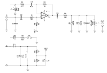
Opamp manufacturers make every effort to minimize bias current in BJT opamps. Let's see how that works in pedal circuit. We'll use the Distortion + (aka DOD 250 OD) as an example. Both of an opamp's input pins must have a DC path to a voltage source. In the case of the + input pin, it's usually a reference voltage. To close the DC feedback loop, the - input pin must have a DC path to the opamp's output pin. R2 is the DC path for the - input. R5, R6 & R7 form the DC path for the + input. Why are R6 & R7 included? Because Vref is not a voltage source. Vcc & GND are voltage sources. Let's assume for the moment that the bias currents in the + and - input pins are equal. R2 & R5 are equal, therefore it follows that the voltage drops across R2 and R5 are equal. Which means that the voltage drops in the two resistors will cancel and the DC voltage on output pin will be equal to Vref. That's what we want. But it's not quite that simple for two reasons. First, the current flowing in R5 has to flow in R6 & R7, which affects Vref. Since R6 & R7 are so large, that effect is noticeable. Second, the bias currents in the two input pins are never equal. The difference in bias currents is called "Offset Current." Let's run the numbers. The typical bias current for a 741 is 80nA. The typical offset current for a 741 is 20nA. Because R2 & R5 are equal, the bias currents cancel out. The offset currents do not cancel, they add. The round trip resistance thru R2 & R5 is 2M. 20nA x 2M = 40mV. This means that the output will typically be around Vref ±40mV. No big deal. The worst-case offset current is 500nA. 500mA x 2M = 1V. This is enough to upset the symmetry in the opamp clipping, but it's unlikely that we will ever find a "worst-case" opamp. Now let's account for the bias current affecting Vref. The parallel resistance of R6 & R7 is 500K. The bias current pushes Vref up or down by 80nA x 500K = 40mV. We can't count on this 40mV to cancel the offset current effect because their polarities might be the same. This means the opamp's output could be (typically) as much as 80mV away from 1/2 Vcc. Not a big deal. The worst-case bias current is 500nA, which would push Vref and the opamp's output voltage by 250mV.
Still with me? That was the hard part. Now let's look at offset voltage. This is easy because C3 blocks DC current. That means at DC, the opamp's gain is unity. Perfect. The input offset voltage, typically 1mV, moves the output 1mV away from Vref. But what would happen if we jumpered C3? Then the opamp's DC gain would be 214x when GAIN is dimed. Now the output would be typically 214mV away from Vref. The worst-case offset voltage is 6mV, which would cause the output to be 1.3V away from Vref. Good thing C3 is there.
The bottom line here is that we need to think about the size of the feedback & bias resistors with respect to opamp selection when designing or modifying pedals.

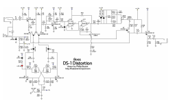
Last thing, we'll talk a little bit about common-mode range. In most pedal circuits, the opamp's inputs don't get anywhere near the rails. In the example above, a 1Vp-p guitar input would drive the inputs to Vref ±0.5V = 4V to 5V. No biggie. Let's see what happens inside the DS-1. Q2 has enough gain that it can be driven to saturation (collector voltage approaches GND) and cutoff (collector voltage approaches Vcc). That means that U1A's + input can be driven very close to the rails. D8 is there to prevent the input from being driven more than one diode drop below GND. The common-mode input range of the M5223 is 0.3V below GND to 1.5V below the positive rail. Clearly, this range can be exceeded in the DS-1. While this apparently does not damage the opamp, it probably contributes to the characteristic distortion that takes place when the opamp is overdriven. The much sought after original MIJ DS-1 used a TA7136 opamp. The Toshiba datasheet says nothing about common-mode input range. This internal input structure is significantly different from the M5223, so one would expect the two opamps to behave differently when the inputs are overdriven.

In an ideal opamp,
1. The current flowing in or out of the input pins would be zero.
2. The voltage difference between the input pins would be zero when the opamp's output is halfway between the rails.
3. The opamp would work correctly even if the inputs are at either of the rails.
With #1 we can get pretty damn close to zero if we use a JFET or MOSFET input opamp. TL072 and CA3130 are examples. While very low input current is not always mandatory, it does make biasing easier. Current flowing in or out of the input pins is called "Bias Current."
The input voltage difference described in #2 is called the "Offset Voltage." It can interfere with biasing if we're not careful.
Most opamps will work as expected if the inputs stay at least 2V below the positive rail and 2V above the negative rail. Operating outside that range can cause the opamp to do things we don't want. The input voltage range limitation described in #3 is called the "Common-Mode Input Range."
Opamp manufacturers make every effort to minimize bias current in BJT opamps. Let's see how that works in pedal circuit. We'll use the Distortion + (aka DOD 250 OD) as an example. Both of an opamp's input pins must have a DC path to a voltage source. In the case of the + input pin, it's usually a reference voltage. To close the DC feedback loop, the - input pin must have a DC path to the opamp's output pin. R2 is the DC path for the - input. R5, R6 & R7 form the DC path for the + input. Why are R6 & R7 included? Because Vref is not a voltage source. Vcc & GND are voltage sources. Let's assume for the moment that the bias currents in the + and - input pins are equal. R2 & R5 are equal, therefore it follows that the voltage drops across R2 and R5 are equal. Which means that the voltage drops in the two resistors will cancel and the DC voltage on output pin will be equal to Vref. That's what we want. But it's not quite that simple for two reasons. First, the current flowing in R5 has to flow in R6 & R7, which affects Vref. Since R6 & R7 are so large, that effect is noticeable. Second, the bias currents in the two input pins are never equal. The difference in bias currents is called "Offset Current." Let's run the numbers. The typical bias current for a 741 is 80nA. The typical offset current for a 741 is 20nA. Because R2 & R5 are equal, the bias currents cancel out. The offset currents do not cancel, they add. The round trip resistance thru R2 & R5 is 2M. 20nA x 2M = 40mV. This means that the output will typically be around Vref ±40mV. No big deal. The worst-case offset current is 500nA. 500mA x 2M = 1V. This is enough to upset the symmetry in the opamp clipping, but it's unlikely that we will ever find a "worst-case" opamp. Now let's account for the bias current affecting Vref. The parallel resistance of R6 & R7 is 500K. The bias current pushes Vref up or down by 80nA x 500K = 40mV. We can't count on this 40mV to cancel the offset current effect because their polarities might be the same. This means the opamp's output could be (typically) as much as 80mV away from 1/2 Vcc. Not a big deal. The worst-case bias current is 500nA, which would push Vref and the opamp's output voltage by 250mV.
Still with me? That was the hard part. Now let's look at offset voltage. This is easy because C3 blocks DC current. That means at DC, the opamp's gain is unity. Perfect. The input offset voltage, typically 1mV, moves the output 1mV away from Vref. But what would happen if we jumpered C3? Then the opamp's DC gain would be 214x when GAIN is dimed. Now the output would be typically 214mV away from Vref. The worst-case offset voltage is 6mV, which would cause the output to be 1.3V away from Vref. Good thing C3 is there.
The bottom line here is that we need to think about the size of the feedback & bias resistors with respect to opamp selection when designing or modifying pedals.

Last thing, we'll talk a little bit about common-mode range. In most pedal circuits, the opamp's inputs don't get anywhere near the rails. In the example above, a 1Vp-p guitar input would drive the inputs to Vref ±0.5V = 4V to 5V. No biggie. Let's see what happens inside the DS-1. Q2 has enough gain that it can be driven to saturation (collector voltage approaches GND) and cutoff (collector voltage approaches Vcc). That means that U1A's + input can be driven very close to the rails. D8 is there to prevent the input from being driven more than one diode drop below GND. The common-mode input range of the M5223 is 0.3V below GND to 1.5V below the positive rail. Clearly, this range can be exceeded in the DS-1. While this apparently does not damage the opamp, it probably contributes to the characteristic distortion that takes place when the opamp is overdriven. The much sought after original MIJ DS-1 used a TA7136 opamp. The Toshiba datasheet says nothing about common-mode input range. This internal input structure is significantly different from the M5223, so one would expect the two opamps to behave differently when the inputs are overdriven.

Last edited:

