fig
Village Idiot
It's kind of a side goal. That and building a shortwave rig. Oh, and cutting a platinum album in there somewhere.Wait…that 8031—are you building a computer?
")
It's kind of a side goal. That and building a shortwave rig. Oh, and cutting a platinum album in there somewhere.Wait…that 8031—are you building a computer?
Got me curious though. I wonder if there's a way to convert an SMD chip to a through-hole...something that can be inserted into a socket.
Here's a one-of-a-kind prototype...nobody steal this one alright?
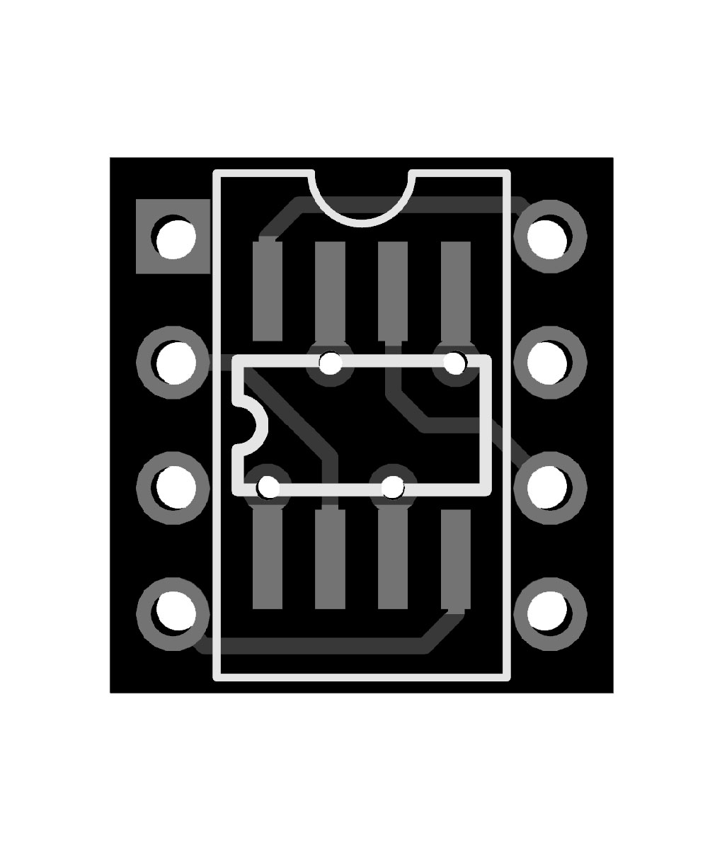
You combine these two ......

...and create......
a DIP-8 2 SOIC-8 2 SOIC-8 2 DIP-8. Genius!

You have to put the thing in the thing and then jiggle the other thing and that thing gets all messed up and....oh f#$% it!That's crazy talk!
You'd have to mate the SMD chip to a SMD-to-THD adapter, then you'd have to solder another THD-to-SMD adapter to the SMD pads on the PedalPCB circuitboard just so you can plug in the SMD IC to the circuitboard. Why not just solder the SMD IC to the SMD pads on the PedalPCB board directly?

Lat summer I went from using paint.net (yes I know, the shame) for the past couple years to Affinity and Illustrator. If I can do it, anyone can. Once you get past the initial learning curve its pretty easy. How far you decide to take it is up to you. With just minimal learning you can do the cookie cutter clip art graphics or learn more in depth controls and start making some really complex designs. The biggest thing I recommend is having templates set up for each enclosure size to cut down on repetitive task so you can spend more time on your designs. Like I said, if my dumbass can do it, you can too.
might not be a relevant question but can you use these stencil with conventional iron/solder or is it ment to be used with solder paste/oven?Diving into SMD has brought many gadgets into play. Test/burn-in sockets for breadboarding, Hot-air stations, infrared rework ovens, solder paste and microscopes, etc. The newest addition is dull as dishwater, but exciting as ice cream......brb.......okay, so passives are passé' and a little dab with the syringe on each pad and pow (at least where 0803/0605 are used). ICs are a bit different. Drag soldering works well, but sometimes leaves a few bridges to be burned.
I bought a couple of stencils to give a try. I'm sure all of you know how stencils work, but I'll show you anyway because I already took the pictures, so pay attention!
One SOP-28 SS stencil courtesy of Proto-Advantage and one SOP-28 CH341a.
Fit's fine...just fine.
Now you just align it over the pads...secure with a bit of kapton and you're ready to smear.
Next up....a break...then...swab the deck me hearties.
I'm struggling to visualize that...help me out.might not be a relevant question but can you use these stencil with conventional iron/solder or is it ment to be used with solder paste/oven?
")
I'm just thinking of those times when you're trying to find a THD component but can't find anything but the SMD equivalent. So, yeah, SMD to THD adaptor for the win. Works for SMD transistors...why not for something like 8-pin SMD chips?
if you are struggling to visualize that ... it's probably that these is no use for it with the purpose I had mind!!!!I'm struggling to visualize that...help me out.

I wouldn't use me as a litmus test. Besides, I haven't had any breaks yet. What's cooking in the cranium?if you are struggling to visualize that ... it's probably that these is no use for it with the purpose I had mind!!!!
I was wondering if the stencil can be as a mask to get a cleaner solder using a conventional iron and 60/40 solder when soldering let's say a FV-1 chip ... probably not what it was intended for...if you are struggling to visualize that ... it's probably that these is no use for it with the purpose I had mind!!!!
#1 in the #2 business!Ahhh it makes sense now. All those breaks are to do a number two...
The Vay Say is a great place to get some thinkering done.
Can't wait for a report back
I know of two ways to find out;
1. Google it and have your hopes dashed to pieces by the over-saturation of misinformation.
2. Try it and see.
I think I'll do a #2.....then try the second one.Stay tuned!
Now I feel stupid.

Now I feel stupid.
Why?Now I feel stupid.
Cause I should have noticed this sooner.Why?
It was a great idea with an incredibly fast turnaround time from Mr PPCB...


