PCB design challenge #1

Missed that! Thanks for the heads up. I'll see if I can fix that up on the schematic and board. :D

Edit: Okay - was a super easy fix... thanks again... don't know how I missed that the first time...

View attachment 48453
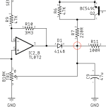
Updated board!

View attachment 48454
Looks great! Judging by looks, this board appears destined for professional manufacturing, but if you were doing this for DIY, you may want to consider increasing trace widths and your clearances a little bit.
 
Looks great! Judging by looks, this board appears destined for professional manufacturing, but if you were doing this for DIY, you may want to consider increasing trace widths and your clearances a little bit.
It's just for me... and I'm pretty fastidious when I'm soldering... :D
 
By DIY, I meant etching the board at home. With small traces and even smaller clearances (trace/ground plane separation), DIY PCB fab may prove tricky. Not judging your soldering ability at all in my statements.
Oh yeah, this isn't homebrew etch by any stretch of the imagination... :D
 
So I finally got around to having these boards made up and could not get it to work. Further inspection of the schematic I used I quickly spotted the error. I completely missed the rectifier feedback resistor which will in turn result in no gain. Easily fixed by kludging the 3M3 on the back of the board but to my main point of this message..... I should not have won this contest!!! I would like to buy (or just send funds to buy) some PCB's from PPCB to
1) @Brett
2) @swyse
and whomever was #4. @temol could you possibly look into that for me and let me know who to contact? I think it might of been @HomebrewTJ
I will also send these folks one of the PCB's that I received that you will have to kludge in R10 but its easy to do.

Thanks everyone,
Lani
 
Last edited:
Big of you to offer this and own up to a small mistake! I never got around to making my board so it could have a mistake too, who knows haha. I only speak for myself here, but I’m very content with what I received for my efforts and don’t feel like I need compensation in anyway, although I do really appreciate the gesture. Just recently I put vbias to an op amp instead of vcc and had to do a cut and run a jumper so I know just how easy it is to make a small mistake on a schematic!
 
Man this contest was some of the most fun i had and in the end I failed. I took so much away from this experience and i wouldn't have it any other way. @Chillums you're brave for letting us know but in reality i think you earned that spot just as much everyone else earned theirs. I just went back and looked at your board design and my memory served me correct, that you 100% earned that!
 
I should not have won this contest!!!
So... funny story... I goofed up on this one as well.

In the process of updating this project from Eagle over to KiCAD, I found a mistake in my schematic. Somewhere between drawing the schematic and dragging components around in Eagle, I inadvertently formed a junction where I shouldn't have. My apologies for not more thoroughly reviewing my files at the time of submission.
 

Attachments

  • quark_oops.png
    quark_oops.png
    130 KB · Views: 6
Back
Top