Bad traces: PCB defect, soldering technique issue, or???

MattG

Well-known member
I finished up an Informant Overdrive build this weekend, and… it didn’t work. Bypass worked, and this circuit has buffered bypass, which means at least part of my work was ok. When engaged, it was almost silent. If I cranked the volume and gain, I could hear the slightest sound.

Tonight I tracked it down to a bad trace on the PCB. I measured an open circuit between two components connected by a short trace. The trace is visible, and didn’t look damaged in any way. Both ends of the trace were “virgin”, meaning there was no re-work involved (when trace damage is much more likely). I soldered in a little jumper wire, and now everything works fine. (I’ll post a build report with pics shortly.)

This isn’t the first time this has happened to me - it also happened recently on one of my own custom PCBs. I feel like, neither my custom PCBs nor PedalPCB uses too-small traces that are right on the edge of manufacturing tolerance. And in both recent cases of this issue, the traces are quite short and direct.

So it’s making me wonder if it’s possible that there is an issue with my soldering technique. I’d like to think it’s good, but issues like this give me pause.

So I’m just putting a feeler out there: how often do you run into bad traces on PCBs (in general, not strictly talking PPCB boards)? Is this just something that happens occasionally, or is it more likely caused by soldering or assembly technique (or lack thereof)?

Edit: Here's the Informant build report, and here's another build report where I had essentially the same problem (on a custom PCB), both have pics of the jumper fix.
 
Last edited:
I've had two bad traces I think - one was a PCBGuitarMania board I bought pre-built because it didn't work, so that could be chalked up to something the builder did. It didn't look like it was reworked or otherwise bad, but who knows. I also don't trust PCBGM so could be a design issue (well, it's not a common issue so the trace is there most of the time, but could be too small or risky or what have you).

The other one was a PPCB Sugarbag Overdrive. I'm fairly sure it was not my fault, but again, you can never know - there was a bunch of resoldering and reworking involved before I found out there was a bad trace, so it could be my fault, but since it was probably what caused the need for reworking in the first place, I would suspect not.

That being said, I've built over 80 pedals total, and from a guess maybe 50 were PPCB pedals? So it's a very rare thing in general. AFAIK manufacturing is very reliable, but of course issues can still happen - I'd probably chalk it up to that for the most part. I'm not sure if they are always tested after manufacturing, but even if they are, it could be that the trace was just weak enough that it gave up during transport or normal soldering.
 
I've never found a bad trace in (assuming) 200+ builds. There are a good number which didn't work, but usually that's PEBKAC.

I can understand a low performing trace getting through the QC though.
 
I had a whole batch of boards (Bathtub Reverb) that had a bad trace on one connection. It was connected in my CAD software, it looks like it was connected on the boards, but it measured open on continuity test. JLC gave me a $4 coupon to make up for it :rolleyes:
 
Shit, guys. Gotta big box coming and you're freaking me out.

This is one that's never happened to me. So far all my errors are homegrown.

One cause of failure I know of is sharp angles in a trace. The etch can build up in the angle and take too much copper. I don't know about KiCad or Diptrace, but the rounded curve traces in EasyEDA are very simple to use.

I can't see under the jumper wire in your build report pic, but what I can see of the trace doesn't look like it should have any problems like that.
 
(...) So it's a very rare thing in general. AFAIK manufacturing is very reliable, but of course issues can still happen - I'd probably chalk it up to that for the most part. I'm not sure if they are always tested after manufacturing, but even if they are, it could be that the trace was just weak enough that it gave up during transport or normal soldering.

I thought that every trace is tested. I watched the QC test on a JLC vid.

Agreed, and that's why I feel like this is more likely something I'm doing wrong.

I've never found a bad trace in (assuming) 200+ builds. There are a good number which didn't work, but usually that's PEBKAC.

I can understand a low performing trace getting through the QC though.

I had to look up PEBKAC - Problem Exists Between Keyboard and Chair. AKA an "ID-ten-T" error (ID-10-T - idiot). I would like to say this is the first time I've had a PEBKAC. I'd even be happy to say this was only the 1000th time I've had one of those!

Did it happen around a large component lead? One of the most common places for a bad trace/pad is around a component with fat leads like a 1N5817 diode.

In this case, it was the trace on the Informant between C4 (22nF) and R6 (1k) - I wouldn't consider either of those to have fat leads.

I always worry about cutting the excess leads and solder blobs on the ground side of big filter caps. Even with the thermal reliefs, I can tell the PCB ground plane is absorbing a lot of the heat, and I'm always anxious about cold solder joints and/or ruining the solder joint when I clip off the excess.

as it turns out, snipping off the excess component lead(s) too close to the thru-hole can damage/sever continuity to the thru-hole.

That's good to know, and seems like the best explanation at this point. Before I determined it was the trace, I thought I might have had a cold or insufficient solder joints on C4 (22nF), as, in this particular case, the extra leads/solder were clipped very short, almost looked to be below flush. So my first fix attempt was just adding a bit more solder and re-touching those joints. But I still didn't get continuity to the next component.

Only very recently did I start trying to cut leads flush with the board. I blame @OD is Glorious - the back of his boards are way too clean, it made me want to improve the look of the "dark side" of my builds. :ROFLMAO:

Here's the Informant build report, and here's another build report where I had essentially the same problem (on a custom PCB).

Edit:

This is one that's never happened to me. So far all my errors are homegrown.

I'm fairly sure this is a homegrown error. I mean, I've done enough work that the odds are a bad trace is bound to have bit me by now. But (at least) two in only a couple months smells more like operator error.

I can't see under the jumper wire in your build report pic, but what I can see of the trace doesn't look like it should have any problems like that.

The trace actually isn't under the jumper wire, it's to the right of my jumper, between those two component leads. It's super short, and only has a couple soft bends. It doesn't look obviously damaged in any way. But the same can be said of the other build I had with a similar issue.
 
Last edited:
That's good to know, and seems like the best explanation at this point. Before I determined it was the trace, I thought I might have had a cold or insufficient solder joints on C4 (22nF), as, in this particular case, the extra leads/solder were clipped very short, almost looked to be below flush. So my first fix attempt was just adding a bit more solder and re-touching those joints. But I still didn't get continuity to the next component.

Only very recently did I start trying to cut leads flush with the board. I blame @OD is Glorious - the back of his boards are way too clean, it made me want to improve the look of the "dark side" of my builds. :ROFLMAO:

The old NASA guidelines specified that leads should be cut before soldering. The idea being that cutting a lead could compromise a solder joint.
 
The old NASA guidelines specified that leads should be cut before soldering. The idea being that cutting a lead could compromise a solder joint.

That certainly makes a lot of sense. Also (slightly) less thermal mass to absorb heat. Doing that will increase my build time dramatically... I usually go through and stuff all or at least most of a component class (e.g. all resistors) at once, using the extra lead length to hold them in place. Then I go through and solder all the connections in one go.

Do you (rhetorical you, anyone reading this) actually do that? Place-clip-solder each component one-by-one? Now I feel like I have to do that. 🥴
 
We also clip before soldering in aerospace because the solder can then flow over the exposed trimmed lead, protecting it from oxidization. I've never watched our techs here do through-hole components, but I assume that's still how it's done.

IPC J-STD-001 (industrial standard, less stringent than aerospace) allows clipping the lead after soldering, but for high-reliability it requires inspection of the joint under magnification and/or reflow of the joint after clipping.
Do you (rhetorical you, anyone reading this) actually do that? Place-clip-solder each component one-by-one?
I've definitely never done it. I don't enjoy through-hole soldering and I do everything possible to speed up the process.
 
That certainly makes a lot of sense. Also (slightly) less thermal mass to absorb heat. Doing that will increase my build time dramatically... I usually go through and stuff all or at least most of a component class (e.g. all resistors) at once, using the extra lead length to hold them in place. Then I go through and solder all the connections in one go.

Do you (rhetorical you, anyone reading this) actually do that? Place-clip-solder each component one-by-one? Now I feel like I have to do that. 🥴

I've done it a few ways. One trick I tried was gluing little pads on my flush cutters to make them "not quite flush cutters." This left a consistent length of lead through the pad. The little pads kept falling off, though.

You can solder resistors from the top, then trim the leads and solder the backside.

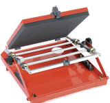
When I was doing production PCBs, I bought an assembly jig that allowed for placing all the components, closing the lid to hold them in place, then flipping it over to solder the backside.

Screenshot 2026-11-17 at 8.50.49 AM.png


I'm on board with @vigilante398 as far as moving to SMD and JLC PCBA. I'll never solder as well as the robot and my time is worth a lot more than what it costs.

I prefer film capacitors in the audio path, so I do those myself.
 
I've had problems when I clip off my leads too short - such that I'm also trimming into the solder, and if my cutters are angled in just the right way I'll cut into a trace. Now I trim the leads just above the cone of solder and leave it intact. It's not so much to preserve the solder but to keep the cutters away from the board.
 
Interesting - more evidence I'm probably being too aggressive with my lead-clipping.

The real reason I was trying for shorter clipped leads isn't so much for aesthetics, but for making it easier to clean up the flux residue. With "pointy" or rough clipped leads, it makes for a sandpaper-like surface that is hard to clean neatly. Nice, smooth, flush- or nearly-flush clipped leads make for a smoother surface that cleans more easily.

That itself is yet another argument for robot-soldered, automated assembly. I just cry a little when it comes to shipping and tariff costs from JLC's PCB Assembly.
 
That itself is yet another argument for robot-soldered, automated assembly. I just cry a little when it comes to shipping and tariff costs from JLC's PCB Assembly.

Yeah, it's that moment when you get through checkout, your butt puckers and you do breathing exercises because you know the total is gonna be like double what's in your cart.

As for cleaning, what I do is keep a tub of 99% alcohol around to dunk the PCBs and scrub them with a toothbrush.
 
Back
Top