


You are using an out of date browser. It may not display this or other websites correctly.
You should upgrade or use an alternative browser.
You should upgrade or use an alternative browser.
Bring out yer Diptrace
- Thread starter Grubb
- Start date



jessenator
Well-known member
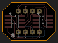
After looking at the price of PDIP TLC2272s (and weeping), I'm coming up with an adapter that can double a "stacked " setup if one wants to channel the Barber mojo, all on as close to a PDIP-8 footprint as I can.

Last edited:
jessenator
Well-known member
Long URL because internet archiveParallel opamps?
The old stacking of opamps for reduced noise deal?
I haven't thought about that in 10 years


Nostradoomus
Well-known member
I believe we called it “piggybacking” back thenI haven't thought about that in 10 years
View attachment 120545


falco_femoralis
Well-known member
Last year I tried working out how to mount everything to one board with the idea of eliminating off board wiring. I worked out that the only kind of jacks that would work are the big neutrik ones that sit recessed inside the enclosure and the nut is a sleeve with threads that goes thru the enclosure holes into the jacks. Those are cool but they're 19mm across and would place the jacks too close together for my liking.
On top of that, I believe a board mounted power jack would not be as robust as an internally nutted (hehe) big style power jack with a big plastic retaining nut. So there is going to be some off board wiring. So I may as well just off board wire the audio jacks too, since it would be like 2 or 3 extra wires max.. yeah?
Instead of that I came up with this system with two boards: one is a daughter board with everything that mates to the top face of the enclosure: all the pots and switches. I made it universal so it can work with any configuration of pots and switches, up to 4 pots and 2 switches. Then there is the main board, which has the audio jacks, circuit, as well as Robert's relay bypass layout. The two boards interface with each other using two right angle pin headers that fit between the boards. Once the pot board is in place, the main board slots into the pin headers and the audio jacks are secured into their holes. Two wires for the foot switch and two more for the power jack. Nice! Four wires!
Here's the back of the pot board. This is what you see when looking into the pedal with the back removed. Two of the pots are piggy backed because this is a 1590b and four pots are pretty much the limit on what I like to put on a 1590b. So the two pots would never be populated at the same time. I used 9mm pots due to the height restraint of the 1590b.

Here's the mating side of the main board. The pin headers here make it so the whole board slides up onto the pot board, and is then secured in place with the audio jacks. This circuit doesn't need connections for every pot and switch, so I pinned them so I can use smaller pin headers if I only need SPDT connections and 3 pots.

Here's the part of the board you see when opening up the back of the enclosure. There is 2mm space on each side of the audio jacks, enough for interior nuts to place the jacks so they extend just enough so nuts and washers fit on the outside with no thread showing. The backing nuts for the audio jacks allow for fine adjustments forward and back to eliminate strain on the connectors. I'm using these jacks here. I derived the dimensions of the 1590b enclosure using one of the ones on amazon and a set of calipers. I took the minimum dimensions and created a pattern in diptrace for it. As I went I created patterns and components for other parts, like the jacks and some others. I got the connectors to interface with the schematic in a clean way by creating potentiometer and switch components as net ports so I can put the connector in its own place in the schem.
My layout isn't as elegant as I'd like. I tried to keep trace lengths as short and straight as I can but it seems crowded in some parts and sparse in others. I feel a more vertical layout would work better, and I should start at the connectors and work outwards. With this one, I was trying to retain some of a previous layout that I liked, and perhaps I should have let it go. The placement of the footswitch pads is not ideal but to fix it I'll have to redo everything and I ain't about that atm.

So with the two board idea I now have (for this circuit) 24 additional pads to solder, while getting rid of 8 wires (16 connections), not including the extra parts for the relay bypass. Is it worth it? What's the point of anything?
On top of that, I believe a board mounted power jack would not be as robust as an internally nutted (hehe) big style power jack with a big plastic retaining nut. So there is going to be some off board wiring. So I may as well just off board wire the audio jacks too, since it would be like 2 or 3 extra wires max.. yeah?
Instead of that I came up with this system with two boards: one is a daughter board with everything that mates to the top face of the enclosure: all the pots and switches. I made it universal so it can work with any configuration of pots and switches, up to 4 pots and 2 switches. Then there is the main board, which has the audio jacks, circuit, as well as Robert's relay bypass layout. The two boards interface with each other using two right angle pin headers that fit between the boards. Once the pot board is in place, the main board slots into the pin headers and the audio jacks are secured into their holes. Two wires for the foot switch and two more for the power jack. Nice! Four wires!
Here's the back of the pot board. This is what you see when looking into the pedal with the back removed. Two of the pots are piggy backed because this is a 1590b and four pots are pretty much the limit on what I like to put on a 1590b. So the two pots would never be populated at the same time. I used 9mm pots due to the height restraint of the 1590b.
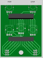
Here's the mating side of the main board. The pin headers here make it so the whole board slides up onto the pot board, and is then secured in place with the audio jacks. This circuit doesn't need connections for every pot and switch, so I pinned them so I can use smaller pin headers if I only need SPDT connections and 3 pots.
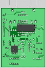
Here's the part of the board you see when opening up the back of the enclosure. There is 2mm space on each side of the audio jacks, enough for interior nuts to place the jacks so they extend just enough so nuts and washers fit on the outside with no thread showing. The backing nuts for the audio jacks allow for fine adjustments forward and back to eliminate strain on the connectors. I'm using these jacks here. I derived the dimensions of the 1590b enclosure using one of the ones on amazon and a set of calipers. I took the minimum dimensions and created a pattern in diptrace for it. As I went I created patterns and components for other parts, like the jacks and some others. I got the connectors to interface with the schematic in a clean way by creating potentiometer and switch components as net ports so I can put the connector in its own place in the schem.
My layout isn't as elegant as I'd like. I tried to keep trace lengths as short and straight as I can but it seems crowded in some parts and sparse in others. I feel a more vertical layout would work better, and I should start at the connectors and work outwards. With this one, I was trying to retain some of a previous layout that I liked, and perhaps I should have let it go. The placement of the footswitch pads is not ideal but to fix it I'll have to redo everything and I ain't about that atm.
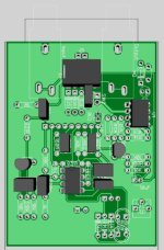
So with the two board idea I now have (for this circuit) 24 additional pads to solder, while getting rid of 8 wires (16 connections), not including the extra parts for the relay bypass. Is it worth it? What's the point of anything?

szukalski
Well-known member

anevilspar7an
Well-known member
I'd be down to buy some if you decide to sell.I recently built some pedals with buffered bypass and it's smooth and quiet enough I've decided to stop using relays altogether.
The I/O PCBs you guys have been doing got be inspired so I thought I'd try one with an Attiny and TMUX4053 electronic switch.
View attachment 123332
View attachment 123333

jubal81
Well-known member
That's pretty hot @jubal81 . Maybe the hottest thing this year.
I love the lack of relay. I hadn't seen the TMUX4053. I've been looking at replacing the MCU in my IO boards with a debouncing IC (MAX6816), replacing the relay as well would be awesome for a minimal footprint!
With the fancy opamp it should be about the same cost as a relay setup.
I've tried another Analog devices debounce IC before and it worked well. They're awful pricey, though.
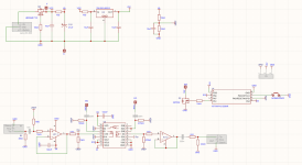
I actually came up with the 4053 scheme earlier this year for a looper-type project I was considering. The three switches ground the input and output of the effect during bypass and programming a 5ms delay between the two control signals should give an imperceptible mute during switching. I showed it to MattG who actually got it working before I did. He says it works great so I'm gonna give it a go.
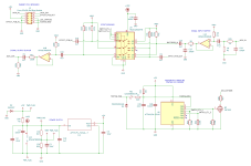
I use essentially the same scheme as what @jubal81 posted in this "quasi-IC" module. I posted the schematic in a similar DIYStompBoxes thread. Schematic attached to this post as well.
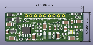
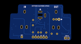
After I posted to DIYSB, RG Keen replied and suggested I consider making it a single-in-line package, using right-angle pin headers. IOW, imagine a little daughterboard that mounts 90-degrees to the main effect PCB (think of RAM modules on a computer motherboard). This is consistent with my "quasi-IC" concept, but it's a better idea because it uses even less board space than my original idea (of mating the buffered bypass PCB directly to the effect PCB).
After RG made that comment, I re-did the PCB layout, and got it down to 43x16mm. But actual consumed effect PCB space would be less than that, basically the size of the 1x9 pin header, plus the overhang on either side. See pic below.
And the next evolution of this will be a double-sided PCB. I'm guessing I can further reduce the width by 30-40%.
I have microcontroller firmware for this here: MCU Firmware for Switch Debounce and Electric Instrument Effects Switching. The following MCUs are supported: AVR Classic (ATtiny13a, ATtiny45, ATtiny85), AVR XT (ATtiny202), PIC10F32x and PIC12F675. For each MCU, three different switching types are supported: mechanical relay (TQ2-L2), x4053 simple, and x4053-with-mute (i.e. what @jubal81 showed above). That means there's 21 released hex images, one for every MCU-switching scheme combination.
My motivation for doing this was because I like to make my own effect PCBs, and I want a Boss-style buffered electrical bypass. Such a bypass takes up a lot of PCB space when done with through-hole parts. I wished there was a plug-and-play IC that did all this. There isn't, so I came up with this. I didn't want to make it an I/O board or standalone bypass PCB (e.g. tied to PedalPCB boards) because I didn't want to constrain it to a specific enclosure or vendor PCB. I wanted it to be lower level, like an IC; a building-block that can be used wherever it fits.
The other upside is that, by going SMD, it opens me up to newer/better parts. The TMUX4053 is SMD-only, but a meaningful evolution of the CD4053. The DG413 is another nice SMD-only analog switch (with slightly better specs than the TMUX4053). And of course, all the SOTA modern audio opamps are SMD-only. Here I'm using the opa1678.
After I posted to DIYSB, RG Keen replied and suggested I consider making it a single-in-line package, using right-angle pin headers. IOW, imagine a little daughterboard that mounts 90-degrees to the main effect PCB (think of RAM modules on a computer motherboard). This is consistent with my "quasi-IC" concept, but it's a better idea because it uses even less board space than my original idea (of mating the buffered bypass PCB directly to the effect PCB).
After RG made that comment, I re-did the PCB layout, and got it down to 43x16mm. But actual consumed effect PCB space would be less than that, basically the size of the 1x9 pin header, plus the overhang on either side. See pic below.
And the next evolution of this will be a double-sided PCB. I'm guessing I can further reduce the width by 30-40%.
I have microcontroller firmware for this here: MCU Firmware for Switch Debounce and Electric Instrument Effects Switching. The following MCUs are supported: AVR Classic (ATtiny13a, ATtiny45, ATtiny85), AVR XT (ATtiny202), PIC10F32x and PIC12F675. For each MCU, three different switching types are supported: mechanical relay (TQ2-L2), x4053 simple, and x4053-with-mute (i.e. what @jubal81 showed above). That means there's 21 released hex images, one for every MCU-switching scheme combination.
My motivation for doing this was because I like to make my own effect PCBs, and I want a Boss-style buffered electrical bypass. Such a bypass takes up a lot of PCB space when done with through-hole parts. I wished there was a plug-and-play IC that did all this. There isn't, so I came up with this. I didn't want to make it an I/O board or standalone bypass PCB (e.g. tied to PedalPCB boards) because I didn't want to constrain it to a specific enclosure or vendor PCB. I wanted it to be lower level, like an IC; a building-block that can be used wherever it fits.
The other upside is that, by going SMD, it opens me up to newer/better parts. The TMUX4053 is SMD-only, but a meaningful evolution of the CD4053. The DG413 is another nice SMD-only analog switch (with slightly better specs than the TMUX4053). And of course, all the SOTA modern audio opamps are SMD-only. Here I'm using the opa1678.
Attachments
jubal81
Well-known member
I tightened up the layout and added a buffered VREF using an ne5532 - one half for the bypass and buffer and the other out to a pad for external use.
The opamp is a basic part and only 12 cents, so I figured - why not?
I also added a slot under the DC jack so if you're using an enclosure-mounted DC jack, you can feed the wires through to the top side. The pinout matches the PPCB layout.
Also found a better PMOS for the polarity protection. HL2309 has much lower RDS(on), takes 60v from drain to source and 20v from gate to source, so I'm skipping the zener.
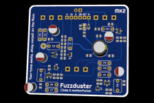
I've been working on a new version of the Fuzzduster so it's the first guinea pig for the connection. Gonna start a separate thread about that effect.


The opamp is a basic part and only 12 cents, so I figured - why not?
I also added a slot under the DC jack so if you're using an enclosure-mounted DC jack, you can feed the wires through to the top side. The pinout matches the PPCB layout.
Also found a better PMOS for the polarity protection. HL2309 has much lower RDS(on), takes 60v from drain to source and 20v from gate to source, so I'm skipping the zener.
I've been working on a new version of the Fuzzduster so it's the first guinea pig for the connection. Gonna start a separate thread about that effect.
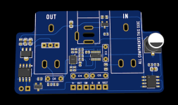
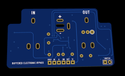
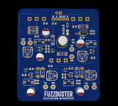
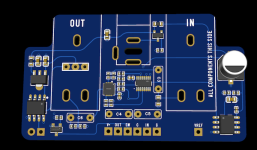
falco_femoralis
Well-known member
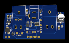
I put together this prototype board mounting everything except the power jack. I'm worried about the durability of a board mounted jack so I'm using a regular big type with a plastic retaining nut.
The view is top down with all components facing the top of the enclosure. I spec'd long leg pots so the jacks and toggle switch will sit at the correct height. The footswitch will sit a bit further in than I normally do but still an acceptable amount.
The pot housings are within the boundary of the enclosure, but I have the enclosure outline on the bottom layer and the 3D modelling projects the outer parts of the board at an extreme angle

This fits a 1590b with side jacks and a 3pdt footswitch. I defined the enclosure outline by measuring an enclosure with a set of calipers and creating a pattern for it in Diptrace. I took measurements of a completed 1590 build to get locations for the pots, LED, and switches. I -think- I have the jacks spaced just the right amount so they should slot perfectly into holes on the sides of the enclosure. I'm thinking I'll tack solder one pin of each into the PCB, then load the board up into the enclosure, insert the nuts and tighten them to set the jacks' angles, and then reflow the tack and solder the rest of the pins once the angles have been established. The jacks come with spacers which according to the data sheets should not interfere with the board edge not being flush with the shoulder of the jack making surface.

With this prototype I want to get an idea of how much I can refine the spacing from the sides of the board to the walls of the enclosure, as well as how the pots, jacks, and switches interface with the enclosure and set the height of the board. There isn't a lot of room so I'd like to learn what the limits are.
The view is top down with all components facing the top of the enclosure. I spec'd long leg pots so the jacks and toggle switch will sit at the correct height. The footswitch will sit a bit further in than I normally do but still an acceptable amount.
The pot housings are within the boundary of the enclosure, but I have the enclosure outline on the bottom layer and the 3D modelling projects the outer parts of the board at an extreme angle
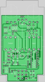
This fits a 1590b with side jacks and a 3pdt footswitch. I defined the enclosure outline by measuring an enclosure with a set of calipers and creating a pattern for it in Diptrace. I took measurements of a completed 1590 build to get locations for the pots, LED, and switches. I -think- I have the jacks spaced just the right amount so they should slot perfectly into holes on the sides of the enclosure. I'm thinking I'll tack solder one pin of each into the PCB, then load the board up into the enclosure, insert the nuts and tighten them to set the jacks' angles, and then reflow the tack and solder the rest of the pins once the angles have been established. The jacks come with spacers which according to the data sheets should not interfere with the board edge not being flush with the shoulder of the jack making surface.
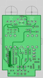
With this prototype I want to get an idea of how much I can refine the spacing from the sides of the board to the walls of the enclosure, as well as how the pots, jacks, and switches interface with the enclosure and set the height of the board. There isn't a lot of room so I'd like to learn what the limits are.
Last edited:
falco_femoralis
Well-known member
I double checked some measurements and made some revisions. Namely the neutrik jack patterns, which were drawn backwards and I needed to correct.

I used the data sheet to verify the jacks dimensions and they were just drawn in the rullywow library with the wider box that is meant to represent the input nearest to the pins for the tip of the TRS cable. I swapped that around and then widened their pin holes in case I need an extra mm of side to side movement when building the pedal.

I sent it off to production and now get to wait two weeks
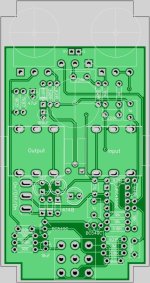
I used the data sheet to verify the jacks dimensions and they were just drawn in the rullywow library with the wider box that is meant to represent the input nearest to the pins for the tip of the TRS cable. I swapped that around and then widened their pin holes in case I need an extra mm of side to side movement when building the pedal.
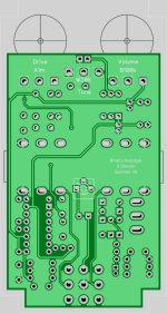
I sent it off to production and now get to wait two weeks
falco_femoralis
Well-known member
Power is all on the bottom plane except for one trace, and audio is all on the top plane except for fiveBe careful with everything on the same plane.
Big Monk
Well-known member
Power is all on the bottom plane except for one trace, and audio is all on the top plane except for five
I mean mechanical components all on the same board.
I understand the allure but it’s a gamble tje more components you board mount.