Buffer + Bypass "Quasi-IC" Module

MattG

Well-known member
I also posted this to DIYStompBoxes, but it's not getting much attention over there, so I thought I'd see if it piqued anyone's interest here.

In my pedal builds, for bypass switching, I generally prefer a buffered electrical bypass scheme (similar to typical Boss pedals). I've been doing this with a CD40106 for footswitch response and state management, and a CD4053 for the actual audio signal switching. I've used this circuit as a standalone module as well as directly integrated into the PCB of the effect itself.

Integrating it directly with the PCB is frustrating with through-hole components, because it uses up so much precious PCB space. The standalone module works fine, but I don't like all the added board-to-board wiring.

I got to thinking, the ideal would be if all this functionality was contained in a single integrated circuit. I don't think such an IC exists. Having custom ICs fabricated is unlikely to be accessible to hobbyist budgets any time soon. So I figured the next-best thing is a "quasi-IC", basically a small (i.e. using SMD components), standalone PCB that can be directly-soldered to the actual effect PCB. My other observation is that all the new and improved ICs are generally only available in SMD format.

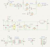
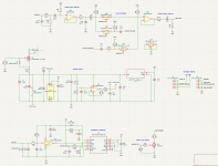
Attached is the design of this "quasi-IC" circuit so far. An overview of the design:
  • TLV9301 for virtual ground buffer: available in ultra-small SC70 package, 150uA quiescent current, can drive capacitive loads
  • AP7375-50 5v LDO: tiny sot-23 package, 3uA quiescent current, up to 45v input voltage
  • DG413 for audio switching: replaces the CD4053 I previously used; quad SPST switches, two normally open, two normally closed; one is unused in this design, the remaining three exactly mimic Boss-style JFET audio switching; 35R on-resistance
  • SN74HCS74 for state-management; this is a dual D (data) flip-flop with Schmitt trigger inputs (think CD4013 with Schmitt inputs); one flip-flop is unused, the other is wired as a T (toggle) flip-flop (/Q tied to D); replaces the CD40106 in my previous design; available in ultra-small SOT-23-THIN package
  • OPA1652 input and output buffers: hifi-grade opamp with super-high impedance JFET inputs, tiny bias current, rail-to-rail capable, overkill specs

In the schematic, the "offboard wiring" will be castellated PCB edges, so the actual effect PCB ("motherboard") would have corresponding solder pads (turning this bypass mini-PCB into a "daughterboard").

The current draft PCB layout is about 38mm X 23mm. Not quite IC sized, but dramatically smaller than the through-hole equivalent.

Any thoughts/comments/criticisms? Notice any errors or gotchas I likely overlooked?

Edits from the original DSB post:
  • I just noticed I have R22 as 22k, that's a typo, should be 22R. (Only off by 1000!)
  • I also realized the input cap C18 plus the R4 Vbias pullup resistor will have a time constant around 10 seconds. I'll think on this a bit, but 1uF or maybe even 470nF is probably fine here.
 

Attachments

  • buffered-electrical-bypass-v3-schematic-20260505.png
    buffered-electrical-bypass-v3-schematic-20260505.png
    68 KB · Views: 12
Here's an updated schematic. I'd like to think I'm getting close to a prototype fabrication run. Changes from the previous schematic:
  • Changed the buffer opamp from opa1652 opa2197; besides being cheaper, the opa2197 is rail-to-rail output and input, and also has some built-in RF protections
  • Put a small RF filter at the circuit input
  • The circuit output now has a 1M pulldown resistor
  • Added p-mos reverse polarity protection (instead of series 1n5819)
  • Added a SN74LVC1G14 Schmitt-trigger inverter on the footswitch (the SN74HCS74 flip flop triggers on a rising edge, so I originally had the footswitch wired directly to the 5v supply; I didn't like this, so in order to tie the footswitch to ground but still have the effect/bypass trigger on a press, I had to drop in an inverter)
  • Several other small tweaks

This is what I have for documentation so far:
  • Power supply: the module assumes the parent PCB has at least 22uF of bulk power supply decoupling
  • The +9v power supply pin is intended for any voltage within 9 to 18 volts
  • The status LED cathode pin has only 4.7k of current-limited resistance; this is provided only for bare-minimum current limiting on this PCB; this is a reasonable value for standard LEDs and 9v operation, but you will generally want to add current-limiting for ultra-bright/high-efficiency LEDs and/or 18v operation.
  • VREF is provided only as a high-impedance bias reference; it should be loaded only with large resistances, preferably 100k or greater; do not use VREF as a supply rail, LED reference, virtual ground power node, or return path
  • The footswitch should be a 2-pin normally-open momentary SPST switch. Connect one pin to FOOTSW and the other pin to the motherboard's 0v/GND. Footswitch leads should be as short as possible (<10cm ideally), and tightly twisted.
  • The footswitch debounce timing is approximately 10-15ms on switch press, and 100-250ms on release (press debounce timing may vary with switch model, age, dirty contacts, etc, as well as actual component tolerances)
  • EFFECT_PCB_IN and EFFECT_PCB_OUT are AC-coupled; the effect must provide its down DC biasing (VREF is available, but cannot be loaded)
 

Attachments

  • buffered-electrical-bypass-v3-schematic-20260511.png
    buffered-electrical-bypass-v3-schematic-20260511.png
    76.9 KB · Views: 8
Cool idea.
Why not just put this on an IO board with jacks?

That's a likely next-evolution of this circuit. Main reason I don't do it now is that I hand-drill my enclosures and I don't feel that my consistency/precision is good enough for an I/O board. Quoting myself from this thread:

I think the next evolution of this idea - and I've seen other people here do exactly this - is to make this quasi-IC into an I/O and power module, where you solder the power and I/O sockets directly to it. Then use a ribbon (or JST) connector to go between the I/O and power module and the actual effect PCB. The only reason I haven't done this myself is that I hand-drill my enclosures - wired I/O and power jacks makes for very forgiving enclosure drill holes. :) But it looks like all the board-mount DC jacks are rectangular, and I don't know how to cleanly make a rectangular hole. So I feel like I'd need some kind of robot-based drilling service to make these precision holes for me to realize such a module.
 
Another vote for the IO board. It removes another component completely from your build, and removes the need for jack in/out pads.

Personally, I don't care about the rectangular hole thing. I just drill an oversize hole for the power, it gets filled by the power cable anyway.
 
Another vote for the IO board. It removes another component completely from your build, and removes the need for jack in/out pads.

But it also removes flexibility... making it into an I/O board basically forces a specific layout. Do you want top-mount 125B, top- or side-mount 1590B, what about 1590A? Etc etc.

The idea is to think of it as an IC for much of your "pedal boilerplate" needs, for use with custom effect PCBs. It will be awkward to use for readily available commercial boards (e.g. PedalPCB, Aion, etc).

So taking the I/O board concept further - why not make the entire effect PCB direct-soldered to I/O and power jacks? That's a big part of the thinking behind this module: it is supposed to facilitate more freedom/flexibility in the PCB design process.

Personally, I don't care about the rectangular hole thing. I just drill an oversize hole for the power, it gets filled by the power cable anyway.

Clearly you're not as neurotic as I am. ;) Even though I know it doesn't really matter, big round hole vs rectangular jack... I'm getting anxious just writing about it!
 
I should also add... I have mixed feelings about I/O jacks being direct-soldered to a PCB anyway. It certainly makes for neat and tidy internals; and it's convenient for building. But the jacks are one of the highest physically-stressed parts of a pedal. So having them isolated from the PCB with physical wires provides some protection for the PCB. It also makes high-wear parts more readily serviceable.
 
So taking the I/O board concept further - why not make the entire effect PCB direct-soldered to I/O and power jacks?
there was a thread a few weeks ago where someone had done that.

I like the idea of yours as a wee IC like plug in module - and possibly common breakout boards with space for it.
 
You can make it compatible with 125B/1590B/1590BB and that covers the majority of use cases. Though you need to compromise on length with 1590B, and clearance can also be a challenge.

It depends on what your use case is, I guess. Mine is for a more enjoyable building experience, so the fewer modules and cables, the better. Add plugin connectors and I’m even happier with assembly!

I’m not sure there’s a problem with durability of onboard jacks. There are plenty of manufacturers doing it, and Ive never heard of it as a common fault.
 
This is an interesting discussion! I had a couple of comments:

- In terms of footprint, using castellated pads is pretty interesting, but it does take a lot of real estate. It might be interesting to try some different layouts - I was thinking of doing something like this with pin headers instead, so you could install this as a stacked board on top of other components to save space. This might remove some of the space constraints as well to let you use cheaper (basic/preferred) components.
- It looks like your BOM is pretty expensive - I'm always looking out for ways to make my stuff cheaper :-)
- could you use a second dual op-amp and use the second half as an inverter (use the inverting input with unity gain) rather than a dedicated inverter chip?
- could you collapse some of your capacitor values? (1u, 4.7u, 10u) to reduce the number of different components? Are you using electros or MLCC caps? (I assume MLCC if you're fitting all of this in 38x25mm!)
- Could you find a way to use the same mosfet type for both the LED switch and the polarity protection (e.g. switching the LED anode to use p-channel, or switching to an N-channel for the reverse polarity protection) Is there something in the JLC basic/preferred catalog that would work instead? (AO3401/AO3400?)
 
This is an interesting discussion! I had a couple of comments:

Thanks for your interest! You're in rare but esteemed company! 🥰

- In terms of footprint, using castellated pads is pretty interesting, but it does take a lot of real estate. It might be interesting to try some different layouts - I was thinking of doing something like this with pin headers instead, so you could install this as a stacked board on top of other components to save space. This might remove some of the space constraints as well to let you use cheaper (basic/preferred) components.

The first run is intended to be installed via pin headers, but that's mostly to avoid un-solder/re-solder if the module needs to be fixed (which it probably will). I was flirting with the idea of having both pin headers and castellated edges, but that worsens the footprint problem. What I decided is, just like with SMD ICs, an adapter board could be created. I.e., direct-solder this module to a slightly-bigger PCB with pin headers. Same answer I have for the "why not make it an I/O module?" question: you can make a mostly-empty I/O module and direct solder this module to it.

My vision is really for this to be IC-like in that it's essentially "bulletproof" - overbuilt/over-engineered for common scenarios, but will survive (or at least be the last thing to fail) in demanding scenarios. So with that framing, consider the scenario with drunk and surly roadies, carelessly tossing equipment around: something connected with pin headers might not survive.

I didn't post here, but you can see the latest schematic and PCB render here: Buffer + Bypass "Quasi-IC" Module Post #10. It's currently 40x23.

- It looks like your BOM is pretty expensive - I'm always looking out for ways to make my stuff cheaper :-)

The actual parts aren't that expensive, IIRC the DG413 switch is the most expensive part, everything else is surprisingly cheap. But many parts are indeed "extended", so yes, on small runs, the $3 feeder fees add up. Current extended parts count stands at 11, so $33 in feeder fees.

I actually started with what you might call a "cost optimized" version of this: giving up small-as-possible footprint, using previous-gen ICs, relaxing the "bulletproof" design goal. And that's essentially what I've been doing with CD4053, CD40106 and TL072. That works totally fine, but... I'm personally willing to pay for what I hope is a state-of-the-art module.

- could you use a second dual op-amp and use the second half as an inverter (use the inverting input with unity gain) rather than a dedicated inverter chip?

In theory yes, but I don't know of any opamps with Schmitt-trigger inputs. Even the CD40106 of the cost-optimized/through-hole version I've been using has Schmitt trigger inputs. I don't want to give that up; combined with the debounce RC network, it's a "belt-and-suspenders" approach to what I hope is switching-never-fails design.

- could you collapse some of your capacitor values? (1u, 4.7u, 10u) to reduce the number of different components? Are you using electros or MLCC caps? (I assume MLCC if you're fitting all of this in 38x25mm!)

It's all MLCC for size. All the caps except the 10uF are basic parts. Some "could" arguably be reduced if I was willing to relax on the overbuilt paradigm. For example, I use those 4u7 caps as AC-coupling caps. The capacitance of MLCC gets derated with a voltage applied. Consider the 18v supply case, the virtual ground (VREF) will be 9v, so those 4u7 could realistically lose half their capacitance. 2uF is still a comfortable margin where bass cutoff shouldn't be a concern.

As for those 10uF parts: JLCPCB actually has 50v 1206 10uF X5R caps as basic parts, but X7R in that footprint is an extended part. Again with the worst-case-scenario thinking, imagine someone playing a hot stage in the summer Arizona sun - the internal temperature of the pedal could exceed 85C (X5R rating) where the performance will likely degrade.

- Could you find a way to use the same mosfet type for both the LED switch and the polarity protection (e.g. switching the LED anode to use p-channel, or switching to an N-channel for the reverse polarity protection) Is there something in the JLC basic/preferred catalog that would work instead? (AO3401/AO3400?)

Both the p-channel used for reverse-polarity protection (AO3401A) and the n-channel for LED (2n7002) are JLCPCB basic parts. The seven ICs I'm using are all extended, along with two specialty diodes (a zener and an ESD diode). That's nine extended parts, the other two are the 10uF X7R caps I mentioned, and - of all things - 2M2 resistors.

All that said, it's still physically bigger than I had hoped when I conceived of this. I don't see a lot of room for further size reduction unless I relax some of the design goals.
 
Clearly you're not as neurotic as I am.
I think the neurosis is there with a different perspective. :LOL: Mine is top-mount in 125B.

The size thing may not be such a problem if the height isn't so bad. People "should" be using low profile parts by default now, since they're readily available.

What package size are you using? You may be able to get away with 0402. Another option, if you disregard the size issue, is using JLC assembly with through-hole for some parts. It's (was?) comparable to extended parts once you include the loading fees etc.
 
What package size are you using? You may be able to get away with 0402. Another option, if you disregard the size issue, is using JLC assembly with through-hole for some parts. It's (was?) comparable to extended parts once you include the loading fees etc.

Here's a direct link to the 20260516 PCB render. All the resistors (except one) are 0603. The caps are 0603, 0805, and 1206 depending on their role. I could probably save a little space dropping down to 0402-sized resistors, but the caps are all deliberately sized.

I think the DG413 (biggest IC) is available in a smaller package... I might try that on a future revision, but at-a-glance, it looks like it would make PCB routing harder. But can't say that for sure until I try.
 
Both the p-channel used for reverse-polarity protection (AO3401A) and the n-channel for LED (2n7002) are JLCPCB basic parts. The seven ICs I'm using are all extended, along with two specialty diodes (a zener and an ESD diode). That's nine extended parts, the other two are the 10uF X7R caps I mentioned, and - of all things - 2M2 resistors.

The 2M2 should at least be 'preferred' (C22938).
There are a bunch of TVS diodes that are basic/preferred also (C2990493 for example), they're under "Circuit Protection" and not "Diodes" of course. There are also a bunch of zener diodes that are 'preferred' and skip the loader fees (e.g. C19077446).

Could you get away with something like a SN74LVC1G74 (C7425509) since you're only using one half of the flip-flop? vs the dual 74hc74, since it's an extended part anyway.

For the switch, could you get away with three tiny SC-70-6's (like C2944066) rather than the DG413? Maybe simplifies routing, too.

If you really wanted to play part golf to keep prices down (at the expense of space) you could parallel two of the 4u7s for 10u also. Or use a TL072 as the vref buffer since those are basic and ~free. Of course this all only matters for small runs -- once you're creating >= 50 of them
at a time you're paying per-bom-part. (at which point you probably have yet different BOM golf games to play)
 
There are a bunch of TVS diodes that are basic/preferred also (C2990493 for example), they're under "Circuit Protection" and not "Diodes" of course. There are also a bunch of zener diodes that are 'preferred' and skip the loader fees (e.g. C19077446).

Both of those examples show up as extended for me, but they are "promotional", I assume that's what you mean by "preferred". Effectively the same as basic, skipping the loader fee. Good idea though - when the time comes to place the order, I might spend some time looking for compatible replacements that are promotional. I've so far only looked at basic/extended because my understanding is that promotional is basically ephemeral, so by the time I actually place the order, they might no longer be promotional. IOW, I feel that's an "optimize at time of order" thing.

Could you get away with something like a SN74LVC1G74 (C7425509) since you're only using one half of the flip-flop? vs the dual 74hc74, since it's an extended part anyway.

Yes, on the updated design I've already switched to that part.

For the switch, could you get away with three tiny SC-70-6's (like C2944066) rather than the DG413? Maybe simplifies routing, too.
That part looks like Shanghai Belling BL1551B. Max voltage supply is 5.5v, and it can only switch up to a bit over voltage supply. So won't work for a signal that is potentially 18v PTP. But that's a good idea though, I might see if there are single analog SPST switches, it would give more routing flexibility.

Or use a TL072 as the vref buffer since those are basic and ~free.

I'm using the TLV9301 single opamp for VREF buffer. $3 feeder fee yes, but: It's ultra tiny (SC-70), a single opamp, specs are better than TL072, and it's stable into a capacitave load... to me, it has virtual ground buffer written all over it!
 
Kicking out some parts I found:

Nexperia Schmitt trigger 74HC14D,653 (BASIC)

OPA1679: Quad opamp in 4X4 QFN package. Rail to rail. CMOS. Audio grade: C1512997

I think the real design challenge with a project like this is how many redundancies you have to engineer into it: Polarity protection, virtual ground rail, multiple buffers.

I just started dabbling in switch ICs and I really like 'em. My vote is go niche and cool. Make it crazy small. Use the extra opamp for an optional boost or line out or something.

Why not just match the pinout at the foot of PedalPCB boards and make it long and narrow so it can be mounted vertically with 90-degree headers?
 
Back
Top