serious, genuine, earnest query:
why not reissue a proper MN3011?
is there just not enough demand for it to be feasible?
i'm seeing ....some?
After being whelmed, but not overly, by the Belton Brick, I thought I'd give a BBD-based reverb pedal a try. I ran across a vintage MN3011 (U3) in my stash and this is what I ginned-up. It's mostly based on an example circuit in the datasheet, with a few extra features thrown in. The MN3011...

forum.pedalpcb.com
After over a year of research, testing, development and prototyping, the Rockman X100 (rev 10) V2 pedal is done. This is the world’s first single-unit full Rockman X100 in a functioning, stand-alone pedal. At this point, only about 40 of the V2 units will be made - still using all the same...
forum.pedalpcb.com
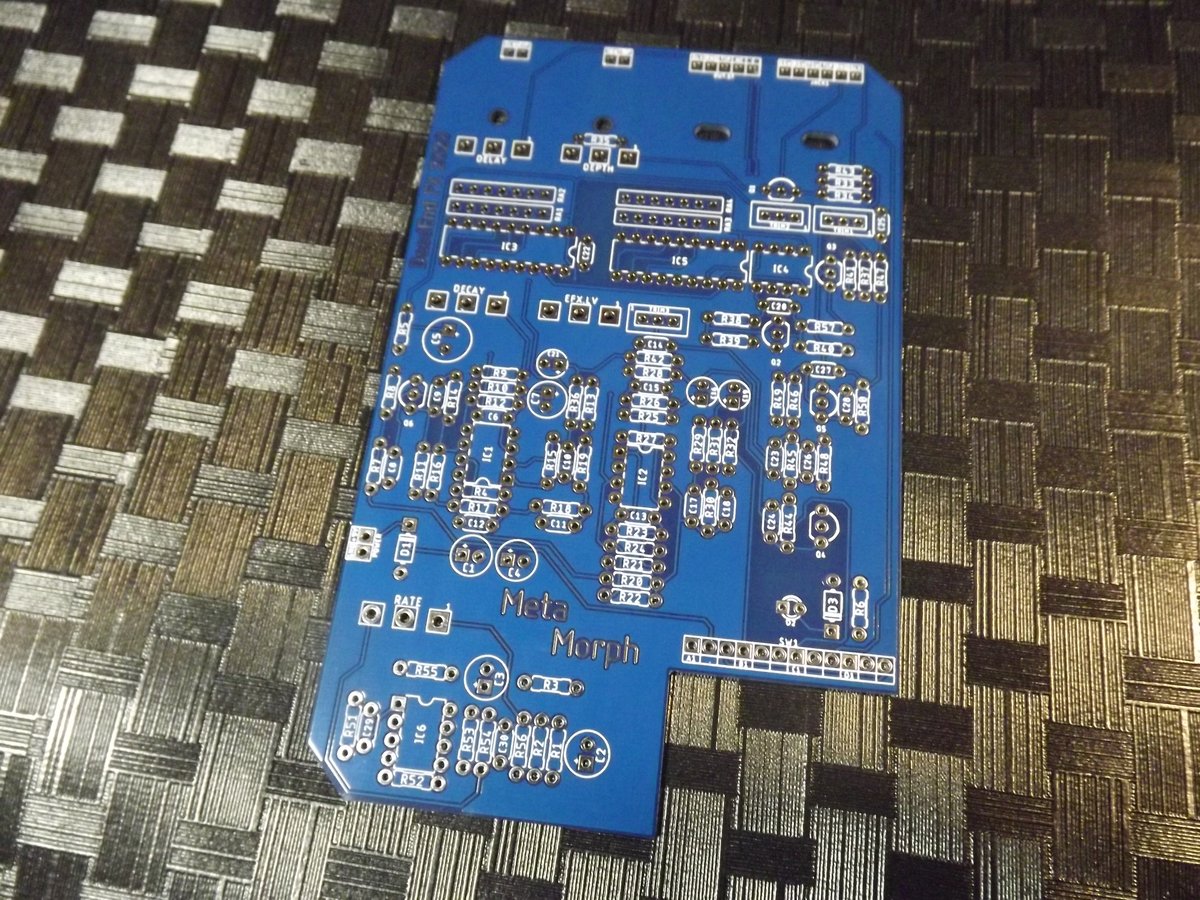
Clone board of the Last Gasp Arts Lab Transroom. Reverb, with a modulation angle. The reverb is along the lines of a plate type reverb, with variable room size and decay. Now add a pinch of modulation to it, with rate and depth control at your finger tips. Top it off with a dry/wet mixer. Delicious!

www.deadendfx.com
i accept that digital has way more capability and potential and makes more sense to invest into, but perhaps if there were reliable sources, maybe the demand would become induced? - just as we've seen lately with all these new BBD devices - boss DM-101, pastfx's catalog, and anyone else trying to jump on the analog modulation train.
i dunno if any of that would have happened without the reissues.
 . . . .