Fat Piggy

beeltink

New member
I built the Fat Piggy, but find the gain so over the top that the pedal just oscillates.
I'm wondering if R7 should be 68k instead of 680k. I just changed R7 and with 68k it sounds much better.

EDIT:
Also R10 could be lower. I went to 47k for R10.
The Gain-pot should also be lower, IMHO, like 100k.

So, my mods:
R7: 68k
R10: 47k
P gain: 100k log (250k log may even be better)
It sounds great now, very 70s stoner rock like, but without all the oscillating.
The gain-switch actually has a use now :)

PedalPCB Fat Piggy.jpeg
 
Last edited:
I think the Oscillation is part of the Design in this pedal.
This PCB has been available around 2 years so any issues would have been corrected.
Maybe someone can chime in on how to tame this Beast!

I think it depends what you're looking for, of course :)
Yet, the gain switch and gain control hardly worked until now, since the input was just way over the top, at least for me.
 
I built the Fat Piggy, but find the gain so over the top that the pedal just oscillates.
I'm wondering if R7 should be 68k instead of 680k. I just changed R7 and with 68k it sounds much better.

EDIT:
Also R10 could be lower. I went to 47k for R10.
The Gain-pot should also be lower, IMHO, like 100k.

So, my mods:
R7: 68k
R10: 47k
P gain: 100k log (250k log may even be better)
It sounds great now, very 70s stoner rock like, but without all the oscillating.
The gain-switch actually has a use now :)
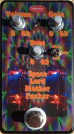
First, it looks great and sounds great!

Next, a few unsolicited comments on the original circuit design and mods...

CD4049s were never intended to be used as analog parts. Consequently, some work better than others. It's always a good move to put them in a socket so you can audition them and select the best ones. Something that PedalPCB did (probably because Pigtronix did it) that is a very bad idea was to leave the inputs on the two unused gates floating. That invites noise and oscillation and leaves the IC vulnerable to damage from static electricity. Unused CMOS inputs should be tied to ground or Vcc. When CMOS gates are biased into linear operation, as they are here, the power supply current is unpredictable. Might be 1mA, might be 20mA. I recommend installing a resistor in series with pin 1, something around 470Ω, to limit the current draw. Then add a separate 100uF bypass cap from pin 1 to pin 8.

As designed, the gain switch selects the 1st stage gain between 2.2dB and 16.6dB. Changing R7 to 68K makes it 0.3dB and 4.5dB. R9 seems way too small to me. That's a good place to dial back the max gain. Try bumping up R9 3x or more, then you can leave R7, R10 and the GAIN pot at their stock values. To maintain the same low-freq response, decrease C12 by the same amount that you increase R9.

My $0.02 ±5%

A very good point about floating CMOS-inputs!
And thanks for the input circuit analysis, I’ll take a look at that as well.
 
Here’s an idea: isn’t it possible to substitute the CMOS with pairs of BS170 and BS250 MOSFETs?
 
Yes, but you'd need at least one additional resistor per stage to limit the drain current. There are plenty of pedals based on discrete MOSFETs. NB: MOSFETs are noisier than JFETs and have lower gain. I have one pedal with a MOSFET input stage (Screw Driver) and it gets noisy at higher PREGAIN settings.
 
First, it looks great and sounds great!

Next, a few unsolicited comments on the original circuit design and mods...

CD4049s were never intended to be used as analog parts. Consequently, some work better than others. It's always a good move to put them in a socket so you can audition them and select the best ones. Something that PedalPCB did (probably because Pigtronix did it) that is a very bad idea was to leave the inputs on the two unused gates floating. That invites noise and oscillation and leaves the IC vulnerable to damage from static electricity. Unused CMOS inputs should be tied to ground or Vcc. When CMOS gates are biased into linear operation, as they are here, the power supply current is unpredictable. Might be 1mA, might be 20mA. I recommend installing a resistor in series with pin 1, something around 470Ω, to limit the current draw. Then add a separate 100uF bypass cap from pin 1 to pin 8.

As designed, the gain switch selects the 1st stage gain between 2.2dB and 16.6dB. Changing R7 to 68K makes it 0.3dB and 4.5dB. R9 seems way too small to me. That's a good place to dial back the max gain. Try bumping up R9 3x or more, then you can leave R7, R10 and the GAIN pot at their stock values. To maintain the same low-freq response, decrease C12 by the same amount that you increase R9.

My $0.02 ±5%
Cheers for insights again, Chuck! Does it simply mean tying the inputs of the two unused stages IC2.1 and 2.6 to ground or also the outputs (pin 2 and 15 respectively) or should the outputs still float? Also, the original comes with 18V power supply as it says they sound better on 18V, is there anything stopping us from putting a charge pump in or could that cause issues like oscillation or stuff?
 
Leave the outputs floating.

I'd be hesitant to run that CD4049 at 18V in linear mode. 9V is already pretty sporting. Higher voltage means more idle current and power dissipation. At some point the IC can't take it any more. 18V might be ok, but I don't recommend it.

My ESR tube amp sounded really good when the power supply caps started to fail, but it didn't last long and took time & money to fix. Just sayin'.
Funny that Pigtronix even include an 18V power supply while saying that it also runs fine on 9V with lesser headroom and volume, more crunch.
Would the current draw of the CD4049 be a bit much for a charge pump? Cheers!
 
Leave the outputs floating.
Input = gnd -> Output = high
Input = Vcc -> Output = low
You could connect the output to either Vcc or Gnd, as long as it is the reverse of the input.
As it is CMOS, current flows during switching/changing the input voltage, AFAIK
 
You are describing the gate's behavior when used as a digital gate. During switching, there is a brief time where both the top and bottom transistors are on. In this circuit, we're not using this device that way. The feedback resistor from output to input biases the gate into the linear region where both transistors are on pretty much all the time. When driven hard, one transistor or the other cuts off, but otherwise, they're both on and conducting current from Vcc to ground. There is nothing in the datasheet to give us any information about how much current will flow under those conditions because the manufacturer does not intend for these gates to be used this way. Feel free to contact an applications engineer at TI if you don't believe me.

It serves no purpose to tie the output of a gate to Vcc or ground. During the power on or power off event, it is common for the output of a gate or opamp to not follow the normal rules. It could slam against either or both rails, potentially overstressing the device.
I’m talking about the non-used invertors. If the input is floating, lots of current could flow, as its state is undefined. If connected to Vcc/gnd it’s high/low, so no current flows through these. The others are used as amplifiers, so current flows constantly, like through a PNP/NPN BJT pair (like a Boss HM-2)
 
Back
Top