Rpschultz13
Well-known member
I’ve studied this guys videos, specifically on grounding. Great stuff, very informative:


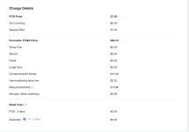
Yeah I have a friend that had a through-hole design he wanted set up for JLC assembly and I was shocked at how much cheaper it was than my usual SMD boards (which admittedly use a large number of weird extended parts).I built a board using through-hole components and wanted to see what the JLCPCB assembly would look like for a purely through-hole board.
For purely through-hole, there's no setup cost and no stencil fee. However, the cost-per-unit for assembly is a lot higher.
For really small runs of boards, I think THT boards would actually be cheaper due to the smaller up-front setup costs.
There's no "Basic vs Extended" juggling because everything is extended but you don't pay a per-extended-part fee
like you do with SMD.
In my example, the boards come out to about $7.50/ea with THT (This is for 5x4-layer boards):
View attachment 105738
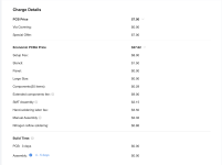
To stack that against a SMT board, here's a board with similar parts count / complexity that is SMT:
View attachment 105739
You can see the $8 setup and $9 in extended fees, but both the assembly cost per board and the component costs are lower.
The component cost for this one is artificially low since some components come out of my pre-purchased parts library.
But I do notice that the SMT parts are significantly cheaper than the THT equivalents.
So anyway, for runs of 5-10 boards the costs will be pretty similar, but for more than that, the lower per-board cost
and lower component costs will quickly offset the setup costs of SMT.
Yeah I've been getting mixed assembly (mostly SMD with through-hole film caps) for a while now, but last month was my first time trying a 100% through-hole board. It's funny how much you save without feeder loading fees, setup fees, stencil fees, etc.I had NO idea you could get thru-hole assembled like SMD.
I had NO idea you could get thru-hole assembled like SMD.
Comment,Designator,Footprint,LCSC,Quantity
10K,"RV1,RV4",RTRIM3362P,C118956,2
Conn_01x03_Socket,"J1,J2",JST_PH_B3B-PH-K_1x03_P2.00mm_Vertical,C131339,2
100pf,"C19,C21,C22,C23",C_0805_2012Metric,C1790,4
1n5819,D1,D_SOD-323,C191023,1
100R,R1,R_0603_1608Metric,C22775,1
15K,R3,R_0603_1608Metric,C22809,1
3.3K,R6,R_0603_1608Metric,C22978,1
4.7k,R12,R_0603_1608Metric,C23162,1Designator,Val,Package,Mid X,Mid Y,Rotation,Layer
C15,2.2nF,C_0805_2012Metric,57.45,-76.85,-90.0,top
C16,2.2nF,C_0805_2012Metric,60.7,-76.85,-90.0,top
C17,2.2nF,C_0805_2012Metric,63.95,-76.85,-90.0,top
C18,100uF,CP_Elec_6.3x5.4_Nichicon,60.1,-70.8,0.0,top
C19,100pf,C_0805_2012Metric,85.9,-73.75,90.0,top
C20,10uF,C_0805_2012Metric,96.05,-65.55,90.0,top
C21,100pf,C_0805_2012Metric,89.3,-75.8,90.0,top
C22,100pf,C_0805_2012Metric,92.625,-75.9,90.0,top
C23,100pf,C_0805_2012Metric,89.3,-72.4,-90.0,top
C24,2.2nF,C_0805_2012Metric,74.05,-85.55,0.0,top
C26,2.2nF,C_0805_2012Metric,96.05,-58.575,-90.0,top
C27,2.2nF,C_0805_2012Metric,92.8,-58.625,-90.0,topThanks for copying all of that. Well, it looks like I'm scuppered, and just need to learn a more modern/supported EDA.The bom looks like:
it'll either get returned or it'll populate 1 of 48 mini PCBs
Does it have to be SMD? JLC also does through-hole assembly, they have plenty of options for through-hole 1uF film caps. That's what I do for caps in the signal path.i'm curious if there are any good SMD choices for 1uF caps in the signal path. should i just go with electrolytic?
I've thought about creating an overlapping footprint with holes for the
through-hole film but also with a SMD footprint for a ceramic I
can have PCBA'd so I can choose later
the conventional wisdom i've seen repeated in multiple places is that C0G/NP0s are fine for the signal path but X7Rs and worse are too unstable in their capacitance to use for the signal path. and C0G/NP0 pretty much only exists in the pF range.(Also I'm not 100% convinced that ceramics are bad in the audio path but I'm half deaf anyhow)
You've heard or even used plenty of circuits with X7R caps in the signal path. One way to minimise the "downsides" is to over spec the voltage of X7Rs and Electros.the conventional wisdom i've seen repeated in multiple places is that C0G/NP0s are fine for the signal path but X7Rs and worse are too unstable in their capacitance to use for the signal path. and C0G/NP0 pretty much only exists in the pF range.
X7Rs are totally fine for a 100nF power filter cap though because that doesn't need to be a perfect value.
