Kliche Mini voltages are not right!

Gt6371

Member
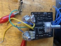
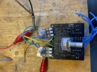
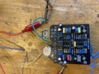
I’ve built several of these and I’ve never had this big of an issue. The voltages on the ICs are way off. I’ve replaced resistors and a capacitor. I’ve checked all solder joints. I just don’t know what else to do. All 3 chips are socketed. I have Kliche that works next to it for comparison. Any help would be appreciated. I’ll try to post pics. I can’t seem to make that work either. Thanks.
Ic1
Pin 1 1.34
1.34
.999
0
9.30
8.57
1.75
.662
Ic2
.88
.488
.489
18.34
17.30
.172
.490
.489
Ic3
9.30
4.99
0
13.48
9.30
1.47
2.56
9.06
 
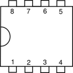
Your numbers make very little sense indeed. Can you confirm that you have numbered the pins according to this diagram?

1657439756261.png

Maybe make a chart like this:

IC1
1 xxxV
2 VVVV
3 YYYv
etc with the pins numbered as per this diagram - this is the standard way that pins are numbered. If your above numbers are in order and correct then it looks as if your power is going to non-power pins of your op amps
 
Your numbers make very little sense indeed. Can you confirm that you have numbered the pins according to this diagram?

View attachment 28665

Maybe make a chart like this:

IC1
1 xxxV
2 VVVV
3 YYYv
etc with the pins numbered as per this diagram - this is the standard way that pins are numbered. If your above numbers are in order and correct then it looks as if your power is going to non-power pins of your op amps
Ic1. 5. 9.30
1. 0. 6. .462
2.0. 7. .408
3.,415. 8. .367
4. 0

Ic2
1..108. 5. 8.69
2..108. 6. .348
3. .457. 7. .351
4. .127. 8. .457

IC 3. Charge Pump
1. 9.30. 5. 9.30
2. 7.60. 6. 0
3. 0. 7. .001
4. 3.48. 8. - .143
 
Ic1. 5. 9.30
1. 0. 6. .462
2.0. 7. .408
3.,415. 8. .367
4. 0

Ic2
1..108. 5. 8.69
2..108. 6. .348
3. .457. 7. .351
4. .127. 8. .457

IC 3. Charge Pump
1. 9.30. 5. 9.30
2. 7.60. 6. 0
3. 0. 7. .001
4. 3.48. 8. - .143
I had all this spaced out I guess it reformats it when I send it. I don’t know how to do charts and all that.
 
OK. IC1 pin 4 should be ground - this is correct
IC1 power pin (8) should be at 9V (or close to). At 0.3V this is way wrong. You are getting (V at pin 5 though. This is way wrong. I would be expecting probably about 4 to 5 V on the rest of the IC1 pins.

IC2 pin 4 is supposed to be -9V, pin 8 is supposed to be 18V. Pins 3 and 5 connect directly to VREF, so they should be sitting at 4.5V.

I think you are still mis-numbering the pins. It looks as if you are numbering them in 2 rows, rather than going anti-clockwise around the IC. If that is the case then you are getting a good ground, and good 9V. First thing then is to get a decent VREF. We will probably need good pictures of both sides of the board. R25 and R26 connect together. The point where they do gives you VREF. Measure the voltages at both ends of those resistors.
I’ll work on this after work today. I’m numbering the pins from top left starting at 1 2 3 4 from top left down then top right 5 6 7 8 going down. I’ll check those voltages and get pics uploaded. Thx for the reply.
 
I’ll work on this after work today. I’m numbering the pins from top left starting at 1 2 3 4 from top left down then top right 5 6 7 8 going down. I’ll check those voltages and get pics uploaded. Thx for the reply.
For the ease of understanding your measurements, please use the pin numberings as in the picture above. Also, your pin 8 (actually pin 5) on the charge pump is definitely wrong as it should measure - 9V.

Please provide pictures of both sides of your board.
 
The numbering of the pins in that picture is the standard numbering used by every manufacturer and every engineer in the entire world. That method of numbering is what we need to be using to make sure that we are all communicating about the same thing.
 
OK now we're getting somewhere, that explains some of the voltages that make absolutely no sense.

Your VREF supply is missing.

Pull out both opamps again (we've communicated by email) but leave the charge pump installed.

Now measure the voltage on all eight pins of both opamp sockets and note the voltages using the pinout posted above. (Pin 1 is the top left pin, Pin 8 is the top right pin)

Be sure to indicate positive or negative voltages.
Well, I feel like an idiot! Lol.
 
Back
Top