Memorial Fuzz (Earthquaker Devices Terminal clone)

PedalBuilder

Well-known member
Build Rating
5.00 star(s)
This is a pretty straightforward and fun build. The Terminal Fuzz is an improved clone of the Shin-Ei Companion Fuzz. The Terminal cicuit incorporates the output boost stage from the General Guitar Gadgets Companion Fuzz and adds two additional controls: a 250k pot wired as a variable resistor in series with the input (Fuzz) and a 10k pot wired in series with one side of the notch filter (voice). The result is a much more versatile and useable take on the Companion Fuzz that still lets you get all of the nasty fuzz tones that put the original Companion Fuzz on the map. I used BC549 transistors from Tayda for all three transistors (hFE ≈ 220). There is some debate as to the correct value for the input capacitor for Q2. The Companion Fuzz used a 47n, but multiple traces found a 4.7n in the Terminal. I tried both, and the 4.7n sounded much better to my ears. The 47n was a lot more muffled and required the treble to be turned at least halfway up before it started sounding good. So if you want a really great 60's style silicon fuzz, grab the Depot Fuzz PCB and go build something. It's easy, sounds great, and doesn't require any exotic components.

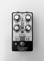
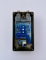
For artwork, I wanted something that shared the appearance of the Terminal Fuzz, but with a local twist as I'm not from Ohio. If you look closely, the PCB layout echoes the artwork. The enclosure is a 125B from Tayda with their matte black sand powder coat, UV printed with two passes of white and matte varnish.
IMG_2732.jpeg IMG_2734.jpeg
 
You have prolific with your own boards lately. I’m sure you have probably answered this before but which program are you using and how long do these take you to design?
I use EasyEDA, which is a browser-based offering from the same entity that owns JLC PCB. I generally do a single board at a time and do the layout slowly over the course of a week or two. Laying out a board usually takes a couple hours in total, but it can take longer, sometimes much longer, if it’s a complex circuit or I want to do something fancy with the layout.
 
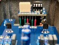
Nice job! How is that relay bypass board mounted?
I use a standard SPST momentary switch. I place the relay bypass board on top of the switch body, and solder the wires to it. The wires hold the board in place very firmly; it doesn't really move even if you pull the microcontroller out of the socket. It doesn't rattle or appear to move when I shake the enclosure vigorously, so it's secure enough for my purposes.

IMG_2740.jpeg
 
4.7n sounded much better to me as well. I read in the forums that people were using 47n and I went that way first. I didn't like it at all. It didn't sound like the original to me.
 
I use EasyEDA, which is a browser-based offering from the same entity that owns JLC PCB. I generally do a single board at a time and do the layout slowly over the course of a week or two. Laying out a board usually takes a couple hours in total, but it can take longer, sometimes much longer, if it’s a complex circuit or I want to do something fancy with the layout.
I have dabbled with EasyEDA a bit and found it to be fairly intuitive to use. Your work is inspiring me to want to make some actual boards with it. I have only designed and made a 3PDT bypass so far. For your boards with the SMD components do you have them install them for you?
 
I have dabbled with EasyEDA a bit and found it to be fairly intuitive to use. Your work is inspiring me to want to make some actual boards with it. I have only designed and made a 3PDT bypass so far. For your boards with the SMD components do you have them install them for you?
Yes, I have all of the SMD components on the relay bypass board and the I/O board are assembled by the fabricator.
 
Back
Top