temol
Well-known member
@perfboarder
Hold your horses, please... your'e not supposed to post any layouts yet. Read the rules.
Hold your horses, please... your'e not supposed to post any layouts yet. Read the rules.
Im sorry. Didnt read first post completely, too excited. Edited post.@perfboarder
Hold your horses, please... your'e not supposed to post any layouts yet. Read the rules.
There are 3 Vcc and 2 Vref locations- should they all be connected somehow? Or is it up to our discretion?

And the grounds- how do you take the ground symbols and connect them? I see how they connect to each component, but then how do you get them off-board?

It's now the 12th where I live so hopefully its submission time,
 so I’ll be watching! I must’ve read the rules incorrectly I thought you had to have a board presentable as well!


That looks awesome. I tried the same thing, but I dig yours.tried to give my board a vintage look, with a bit of modernity
 - 3DPCB - TOP (COMPONENT).png")
 - 3DPCB - BOTTOM (SOLDER).png")

IC power (pin 8) going to VCC. Not 5V.I couldn’t get mine to work
I still want to submit something this is far as i got and the board did not work!
View attachment 40070
View attachment 40071
View attachment 40073
What an experience this was! Im glad to have participated, I learned so much! I ended up using KiCAD as my program of choice. The toner transfer was successful but the board itself does not work! I ended up having to use 5 jumpers.
View attachment 40074
View attachment 40075
View attachment 40076
Im going to take everything i learned here and move onto Buddys contest! Thank you @temol for making the contest but sorry to present you an incomplete piece of work that is not in pdf. format. I have a new found respect for everyone here making these circuits! Thanks for reading!
Thank you so much! Im going to take a look at that right now! Its my first time with KiCAD and my 2nd time doing a toner transfer! So I need to connect Pin 8 of IC to a trace that is VCC! Man i completely messed that up! Very good eye man! Going to see if i can break that trace and create a jumper to VCC! If not ill just try and do it again before the contest ends!IC power (pin 8) going to VCC. Not 5V.
Fix that, and you get working. Nice toner transfer btw. And if your first try on kicad, that awesome!
Almost..
Wow, all above entry 125B.
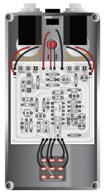
") My board also fits into Gainta BS13. It's between 1590B and 125B.
My board also fits into Gainta BS13. It's between 1590B and 125B.