You are using an out of date browser. It may not display this or other websites correctly.
You should upgrade or use an alternative browser.
You should upgrade or use an alternative browser.
Question About Ground Connections in My DIY Pedal
- Thread starter ori1122
- Start date
rwl
Well-known member
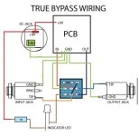
As you can see, the ground is connected to the two audio jacks, the foot switch as the ground for the bypass LED, and the actual ground from the 9V jack.
The PCB probably has a ground plane, connecting all the grounds together, and filling any empty space on the board, it's just not showing it - it's not typically labelled. This would connect with any other grounds for the circuit. As an example, the 7.5K resistor above probably has one pad going to ground as well.
The PCB probably has a ground plane, connecting all the grounds together, and filling any empty space on the board, it's just not showing it - it's not typically labelled. This would connect with any other grounds for the circuit. As an example, the 7.5K resistor above probably has one pad going to ground as well.
JohnnyCreepy
Well-known member
View attachment 106659
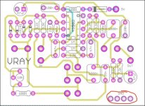
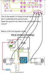
This is the pedal I’m trying to build right now, but I don’t understand the ground part.
Does the ground not need to be connected to any circuit?
Below is the true bypass wiring
View attachment 106660
Got the idea?
ori1122
New member
What I’m curious about is not the wiring, but the fact that the ground pad isn’t connected to any other pad, so I want to know where the copper trace is supposed to be connected.View attachment 106661
Got the idea?
ori1122
New member
I don’t quite understand — does this mean the ground pad should be connected to the 7.5k resistor pad?As you can see, the ground is connected to the two audio jacks, the foot switch as the ground for the bypass LED, and the actual ground from the 9V jack.
The PCB probably has a ground plane, connecting all the grounds together, and filling any empty space on the board, it's just not showing it - it's not typically labelled. This would connect with any other grounds for the circuit. As an example, the 7.5K resistor above probably has one pad going to ground as well.
rwl
Well-known member
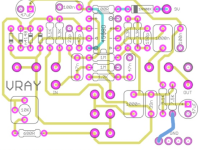
No, it means that they are connected. It's typical on PCB diagrams that ground is treated specially and not actually labeled, because a bunch of components will go to ground. If you have the circuit schematic you'll probably see these components, including the resistor, connected to ground.I don’t quite understand — does this mean the ground pad should be connected to the 7.5k resistor pad?
Basically the "background" of the PCB is typically two thin sheets of copper connecting a bunch of components and the 4 ground pads, it's just not showing it in this image. All of the pads that aren't shown connected to anything are probably connected to these ground sheets.

Here's an example of a different board where you can actually see the ground pour as the faint purplish background. If you look at the four pads at the top of the image you can see little connectors attaching each of the ground pads to the sheets. They're omitted for the 9V pad, since that shouldn't go to ground.
pricklyrobot
Well-known member
I think it’s also useful, conceptually, to differentiate between 0V (the black wire coming from your power supply) and chassis ground.
0V is your return current path, you need it for your circuit to work.
And in a pedal you’ve got a DC power circuit and an AC audio circuit that both need a 0V reference.
The “ground” wires are there to bond the metal parts together, and connect them (ideally at a single point) to the 0V return current path.
In a higher voltage circuit this bonding is done for safety. In a pedal circuit it’s done mainly to direct noise (RF, EMF, and other stray micro-currents) away from your audio path.
Last edited:
ori1122
New member
“I understand completely now. It means the copper plane is widely connected like that, right?No, it means that they are connected. It's typical on PCB diagrams that ground is treated specially and not actually labeled, because a bunch of components will go to ground. If you have the circuit schematic you'll probably see these components, including the resistor, connected to ground.
Basically the "background" of the PCB is typically two thin sheets of copper connecting a bunch of components and the 4 ground pads, it's just not showing it in this image. All of the pads that aren't shown connected to anything are probably connected to these ground sheets.
The green area represents the copper plane
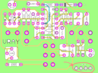
rwl
Well-known member
I think there may be a translation problem for the colors (I wouldn't say there's any green in my image, but I think Japanese labels colors differently). But you probably got it right.The green area represents the copper plane
The two ground planes or sheets are blue and red, and when both are present it's a faint purple color, which is most of the board. In some places there isn't room for the sheet and you'll see only the blue or red (like below Q2).
ori1122
New member
I think there may be a translation problem for the colors (I wouldn't say there's any green in my image, but I think Japanese labels colors differently). But you probably got it right.
The two ground planes or sheets are blue and red, and when both are present it's a faint purple color, which is most of the board. In some places there isn't room for the sheet and you'll see only the blue or red (like below Q2).

The green part was meant to indicate the photo I uploaded
Similar threads
- Replies
- 4
- Views
- 533

