Schematic component order?

Dan0h

Well-known member
I have a question about component layout. I want to build a Green Russian so I can compare it to my original Green Russian and see how close I can get the one I build vs the original. I noticed that the PedalPCB schematic is almost identical to the one kitrae's site but that the Diode clipping loops are placed before the Capacitors instead of after the capacitors C5 & C8 respectively. My question is: Are these moved for a sound benefit, as my understanding on how all this stuff interacts is still NOOB, or are they moved because of another reason? And generally, are pedalPCB boards exact replicas/clones of their influence pedal or are there often slight tweaks to make them unique? Thank you for any info, I am very curious to build my knowledge of all this stuff. Oh and keep up the amazing work, this site and pedal building is so addictive.
 
Some PedalPCBs may have removed buffers like in old DOD pedals or some parts replaced. I believe these are “based on” original. Would you say that the Wampler Tumnus a clone of the Klon Centaur. I believe they use is “inspired”.

For me, my DIY pedals sounds better than the original because I built it. ?
 
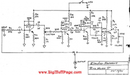
I have seen the schematic drawn both ways, there are even hand drawn EHX schematics depicting them both ways. The following is an example from Kit Rae's pages. So either way is technically correct.
1603301451856.png
 
I have seen the schematic drawn both ways, there are even hand drawn EHX schematics depicting them both ways. The following is an example from Kit Rae's pages. So either way is technically correct.
View attachment 7193
That’s pretty interesting. The placement has to effect the sound right? I really need to dig into how all this stuff interacts with itself. Maybe I need to get a breadboard and start playing around.
 
In regards to this circuit I don't believe it has that much effect. The forward bias resistance is at most 2K so roughly a change of 20Hz with a 100nF cap or 1Hz with a 1uF cap.
 
I have wondered similar things in the past. For example when you have one stage going to another through a cap and a resistor. If there are no other components between the cap and resistor you can change the order of that cap and resistor with no audible effect and that's handy because sometimes it can help you make your layout easier.

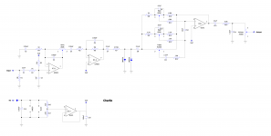
For example:

Charlie Schematic.png

Here I can put C1 after R2 if I wanted, or C5 and R5 could swap places with no affect on the sound. In general I would put the resistor as the connection to the IC though.
 
I have wondered similar things in the past. For example when you have one stage going to another through a cap and a resistor. If there are no other components between the cap and resistor you can change the order of that cap and resistor with no audible effect and that's handy because sometimes it can help you make your layout easier.

For example:

View attachment 7249

Here I can put C1 after R2 if I wanted, or C5 and R5 could swap places with no affect on the sound. In general I would put the resistor as the connection to the IC though.
In this circuit you may be able to get away with swapping C1 and R2 from a tone stand point. You have to look at the components its connected to and the path to ground or the power source. In this circuit R2 and C2 form a low pass filter with a cut freq of 159Khz. So all freq below 159Khz will pass through, freq above 159Khz will be attenuated (this will follow a graph, the higher you go the greater the attenuation, look it up, its a whole other topic). If you swap C1 and R2, now C1 and R3 form a high pass filter with a cut freq of 7.2hz. So all freq above 7.2hz will pass, and freq below 7.2 will be attenuated. Since both freq are outside of the human hearing range you wouldn't hear the changes. But what are R2 and C2 doing in this circuit is the key. R2 and C2, by forming the low pass filter are protecting the op amp from high freq. (This is from the Rat circuit). So swapping C1 and R2 you could expose the op amp from the freq you were trying to keep out of it. So from an operational stand point you do not want to swap these components.

Now with C5 and R5, they would have no change on the freq response of the circuit as they are not forming a filter, but R5 is part of the IC1.2 feedback circuit, which is setting the gain of IC1.2. I've never tried swapping these on an inverting op-amp, so I'm not sure if it will change to op-amp operation. My gut says it will. The gain of IC1.2 = R6/R5, so swapping R5 and C5 may change the gain. Normally this isn't done, the coupling cap always comes before the the resistor in this type of circuit, at least in my experience. Might have to breadboard an inverting op amp and put theory to practice.
 
Last edited:
The rabbit hole keeps getting deeper. I like the idea of getting a breadboard and experimenting, but I would not know things like keeping certain frequencies from certain components. There is a lot to learn. The interaction of all these components is massively interesting. Even more intriguing is how some combinations can make beautiful sounds.
 
The rabbit hole keeps getting deeper. I like the idea of getting a breadboard and experimenting, but I would not know things like keeping certain frequencies from certain components. There is a lot to learn. The interaction of all these components is massively interesting. Even more intriguing is how some combinations can make beautiful sounds.

The rabbit hole is very deep!? I have a background in electronics, but not audio circuits. They are a beast on their on and I am learning something new everyday. You have to look at them in 2 different views. One from the DC bias of the circuit and then from the AC audio side. Then there is always things you don't see, like unexpected parallel paths, they can drive you crazy.
 
I have a question about component layout. I want to build a Green Russian so I can compare it to my original Green Russian and see how close I can get the one I build vs the original. I noticed that the PedalPCB schematic is almost identical to the one kitrae's site but that the Diode clipping loops are placed before the Capacitors instead of after the capacitors C5 & C8 respectively. My question is: Are these moved for a sound benefit, as my understanding on how all this stuff interacts is still NOOB, or are they moved because of another reason? And generally, are pedalPCB boards exact replicas/clones of their influence pedal or are there often slight tweaks to make them unique? Thank you for any info, I am very curious to build my knowledge of all this stuff. Oh and keep up the amazing work, this site and pedal building is so addictive.

Getting back to the original question...

The order of C5/C8 and the diodes does not matter electrically. Whatever makes the layout flow is best.

All that stuff Chas sais is true, especially the part about the Rabbit Hole being deep. Electrical design is usually a compromise between conflicting requirements. Even simple designs can have unexpected nuance.
 
Back
Top